Infrared solid-state imaging device

a solid-state imaging and infrared technology, applied in the field of infrared solid-state imaging devices, can solve the problems of reducing the measurement accuracy of infrared rays, device output may drift along with the temperature change of the device, and the inability to achieve the necessary degree of amplification, etc., to suppress temperature drift and reduce voltage drop in the drive line

Active Publication Date: 2013-04-30
MITSUBISHI ELECTRIC CORP
View PDF7 Cites 4 Cited by
  • Summary
  • Abstract
  • Description
  • Claims
  • Application Information

AI Technical Summary

Benefits of technology

[0013]It is hence an object of the present invention to provide a thermal infrared solid-state imaging device capable of solving the problem of voltage drop in the drive line occurring in mega-pixel structure of the thermal infrared solid-state imaging device (in which, the number of pixels is increased), and suppressing the temperature drift caused by device temperature variations.
[0026]According to the invention, even thought the number of pixels of the two-dimensional pixel array of the thermal infrared solid-state imaging device is increased to be large number (in mega-pixel structure), it is possible to reduce voltage drop in the drive line and to suppress temperature drift due to device temperature variations.

Problems solved by technology

Accordingly, the amplifier may be saturated by the voltage drop distribution by the drive line, and a necessary degree of amplification may not be achieved.
Moreover, the response of the pixel includes a response due to a device temperature change aside from the response of infrared light, and thus the device output may drift along with the device temperature change.
Since the output variation due to this ambient temperature change cannot be distinguished from the change in the incident infrared ray, the measurement precision of infrared ray is lowered, and a stable image cannot be obtained.
In the two-dimensional pixel array of the above thermal infrared solid-state imaging device, if the number of pixels is increased to large number (for example, the number of pixels over 640×480 pixels for the two-dimensional pixel array in the conventional mainstream of the thermal infrared solid-state imaging device), the following problems occur.
However, even though these techniques are used, the increase of the number of pixels expands the voltage drop itself in the drive line, so that it is difficult to assure the input voltage range of the differential integrating circuit more than the voltage of the increased voltage drop in the drive line.

Method used


Image

  • Infrared solid-state imaging device
  • Infrared solid-state imaging device
  • Infrared solid-state imaging device

Examples


first embodiment

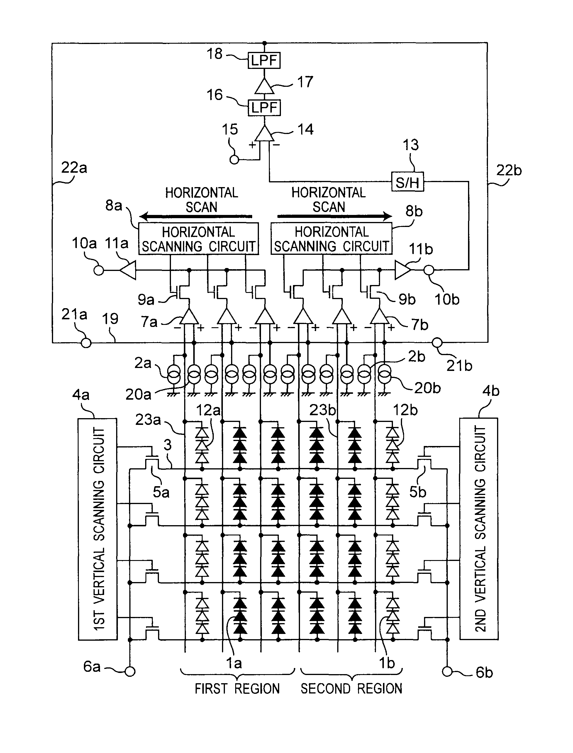
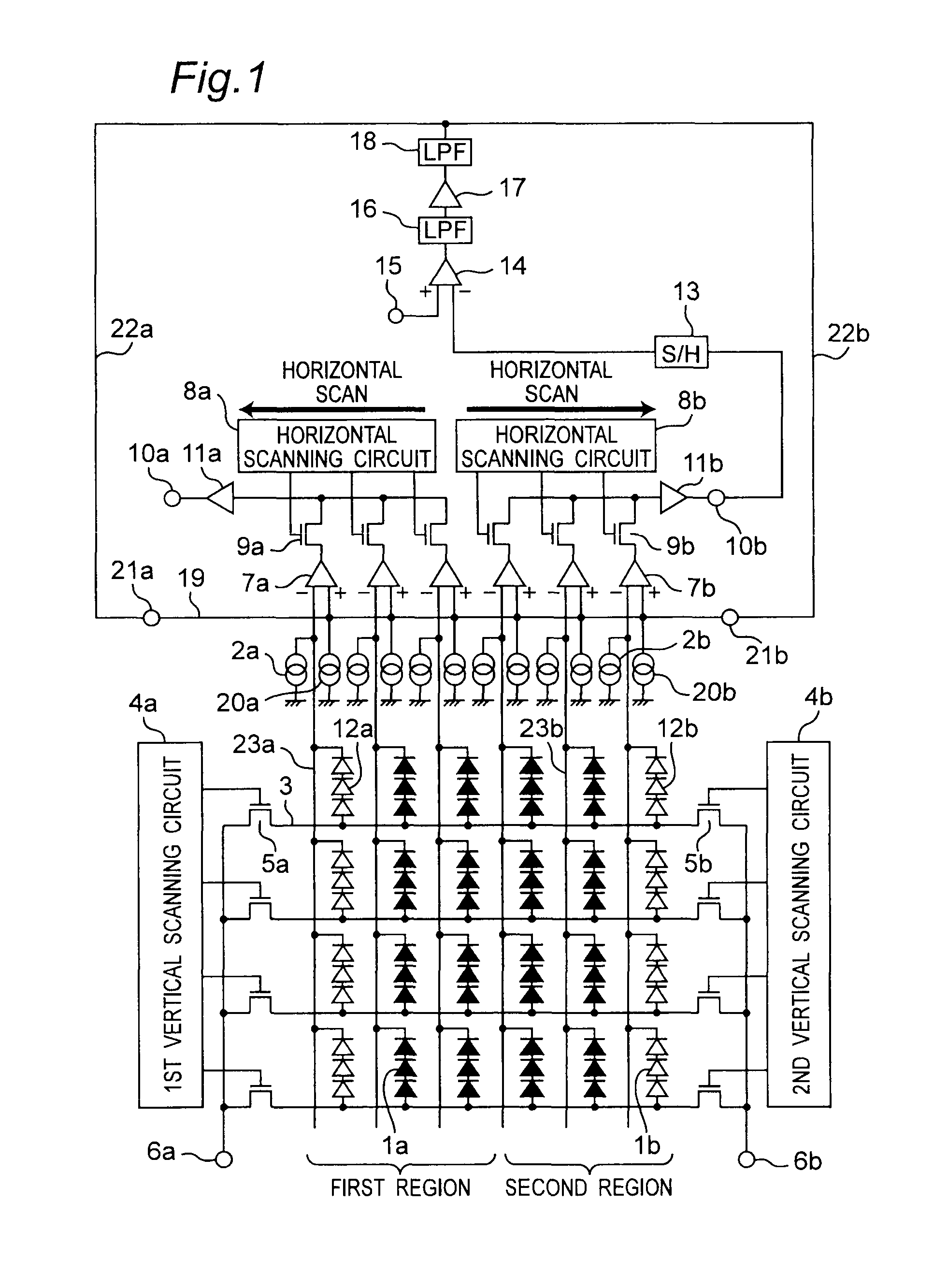
[0042]FIG. 1 is a circuit diagram sowing a thermal infrared solid-state imaging device in a first embodiment of the present invention. In the thermal infrared solid-state imaging device, similarly to the conventional thermal infrared solid-state imaging device, a plurality of diodes each having an infrared ray absorbing structure and a thermally insulating structure are connected in series to form individual photosensitive pixels 1a and 1b. The photosensitive pixels 1a and 1b are disposed two-dimensionally to form a pixel area.

[0043]The pixel area is divided into right and left parts from the middle. The left part of the pixel area is a first region, and the right part of the pixel area is a second region. The number of pixels contained in the first region is preferred to be same as the number of pixels contained in the second region. The photosensitive pixel 1a is a photosensitive pixel formed in the first region of the pixel area, and the photosensitive pixel 1b is a photosensitiv...

second embodiment

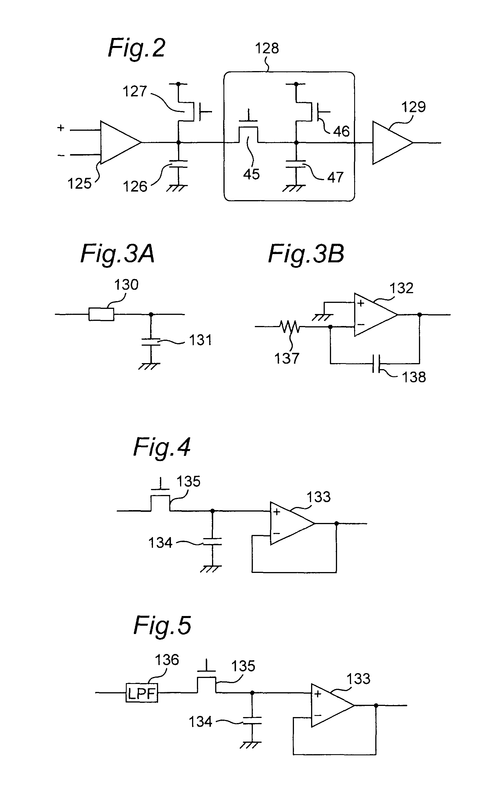
[0083]FIG. 7 is a circuit diagram of a thermal infrared solid-state imaging device in a second embodiment of the present invention. As shown in FIG. 7, the thermal infrared solid-state imaging device of the second embodiment is similar to that of the first embodiment in configuration, but it is different in the following structural points. The configuration and operation different from the thermal infrared solid-state imaging device of the first embodiment are specifically described below.

[0084]As shown in FIG. 7, the thermal infrared solid-state imaging device of the present embodiment is further provided with an analog averaging circuit 24 in addition to the configuration of the thermal infrared solid-state imaging device of the first embodiment. Moreover, in this embodiment, sample hold circuits 13a and 13b are provided to the signals from the first region and the second region of the pixel area, respectively. The input of the sample hold circuit 13a for the first region is conne...

third embodiment

[0094]FIG. 8 is a circuit diagram of a thermal infrared solid-state imaging device in a third embodiment of the present invention. In the thermal infrared solid-state imaging device, same as in the first embodiment, a plurality of diodes having an infrared ray absorbing structure and a thermally insulating structure are connected in series to compose the respective photosensitive pixels 1a, 1b, 1c, and 1d. The photosensitive pixels 1a, 1b, 1c, and 1d are combined to compose a two-dimensionally arrayed pixel area.

[0095]The pixel area is divided into four regions, upper and lower, right and left, from the center, that is, first to four regions. Preferably, the number of pixels included in each region should be identical. The photosensitive pixel 1a is a photosensitive pixel formed in the first region which is the upper left region of the pixel area. The photosensitive pixel 1b is a photosensitive pixel formed in the second region which is the upper right region of the pixel area. The ...


PUM


Abstract

A thermal infrared solid-state imaging device includes a horizontal scanning circuit for scanning a pixel area horizontally to read an infrared image, and vertical scanning circuits provided at both ends of the pixel area. The vertical scanning circuits drive a drive line by applying a driving voltage at both ends of the drive line (in two-end driving). Further a bias voltage is applied at the end of the pixel area to a bias line connected to differential integrating circuits.

Description

BACKGROUND ART[0001]1. Field of the Invention[0002]The present invention relates to a thermal infrared solid-state imaging device for detecting a temperature change generated by an incident infrared ray with two-dimensionally arrayed semiconductor sensors, and more particularly to a thermal infrared solid-state imaging device that integrates electric signals from the semiconductor sensors in a signal processing circuit to outputs a detection signal.[0003]2. Related Art[0004]A general thermal infrared solid-state imaging device includes pixels, each having a thermally insulating structure, which are arrayed two-dimensionally, and captures an infrared image by using a change in temperature of pixels caused by an incident infrared ray. Regarding a non-cooling type thermal infrared solid-state imaging device, as a temperature sensor serving as a pixel, several sensors are known, such as a bolometer which is made of polysilicon, amorphous silicon, silicon carbide, vanadium oxide, or the ...

Claims


Application Information

Patent Timeline
Patent Type & Authority Patents(United States)
IPC IPC(8): G01J5/20
CPCH04N5/33H04N5/3651H04N5/3742H01L27/14669H04N25/671H04N25/767
Inventor ONAKADO, TAKAHIROUENO, MASASHI
Owner MITSUBISHI ELECTRIC CORP
Why Eureka
Try Eureka