Optical low-pass filter

a filter and optical technology, applied in the field of optical low-pass filters, can solve the problems of reducing the light amount of radiation to the object entering the imaging device, capturing the shadows of dirt and dust, and preventing the attachment of dirt, etc., to achieve satisfactory conductivity, suppress the cost, and prevent the effect of dirt attachmen

Active Publication Date: 2013-05-07
SONY CORP
View PDF18 Cites 1 Cited by
  • Summary
  • Abstract
  • Description
  • Claims
  • Application Information

AI Technical Summary

Benefits of technology

[0020]With the optical low-pass filter of the invention, a light of a specific wavelength range is reflected or passed through. A coating layer in which a high-refractive layer and a low-refractive layer are sequentially disposed alternately on one on the other is formed on the surface of the base material, and at least one of the high-refractive layers of the coating layer is made of a transparent conductive material. The configuration can thus achieve, all at once, the coating of reflecting or passing through the light of a specific wavelength range, and the ensuring of the conductivity on the surface of the low-pass filter. This eliminates the need to provide a conductive member separately from a coating member of reflecting or passing through a light of a specific wavelength range, thereby being able to effectively prevent the attachment of dirt and dust to the surface of the low-pass filter while suppressing the cost.
[0021]Moreover, if the outermost high-refractive layer is made of a transparent conductive material, the attachment of dirt and dust can be prevented to a further extent. Further, when the total layer thickness is 140 nm or smaller for the refractive layers formed outside of the high-refractive layer made of the transparent conductive material, the coating layer can have the satisfactory conductivity on the surface, and a simple grounding configuration allows grounding so that the attachment of dirt and dust can be prevented to a further degree.
[0022]Further, if the layer thickness is in the range of 200 to 300 nm for the high-refractive layer made of the transparent conductive material, the light reflex loss can be suppressed on the coating layer while the conductivity is being retained on the surface of the coating layer.
[0023]When the layer thickness is in the range of 140 to 220 nm for the low-refractive layer on the base material side being in contact with the high-refractive layer made of the transparent conductive material, the light reflex loss can be suppressed in the visible light region by the coating layer.
[0024]When the transparent conductive material is a mixture of indium oxide and tin oxide with a mixture ratio of the indium oxide being 90 weight percentage or higher, the light absorption can be suppressed.
[0025]When the outermost low-refractive layer is configured as an equivalent layer at least of two layers of MgF2 layer and SiO2 layer, and when the MgF2 layer and the SiO2 layer are disposed in order from the outside, the result will show excellent solvent-resistance and environment-resistance while suppressing the attachment of dirt and dust. This serves more effects when the layer thickness of the MgF2 layer and that of the SiO2 layer each fall in the range of 20 to 80 nm.

Problems solved by technology

The issue here is that optical devices such as low-pass filter and infrared blocking filter are each made of an insulation material, and thus are easily attached with dirt and dust due to static buildup easily caused by piezoelectric effects and pyroelectric effects.
There is a problem that, when these optical devices are attached with dirt and dust, the shadows of the dirt and dust are possibly captured by the imaging device.
Especially with a camera such as single-lens reflex camera in which the camera lens is exchangeable, it is highly possible that the dirt and dust get into the camera at the time of lens exchange, thereby easily causing the problem as above.
However, if the transparent conductive film is a coating film of metal or others, the light will be reflected on the coating film of metal because the coating film of metal is high in refraction index, thereby causing a new problem of reducing the light amount of the radiation to the object entering the imaging device.

Method used


Image

  • Optical low-pass filter
  • Optical low-pass filter
  • Optical low-pass filter

Examples


Embodiment Construction

[0041]In the below, an embodiment of the invention is described by referring to the accompanying drawings. Note here that the invention is not at all restrictive to such an embodiment.

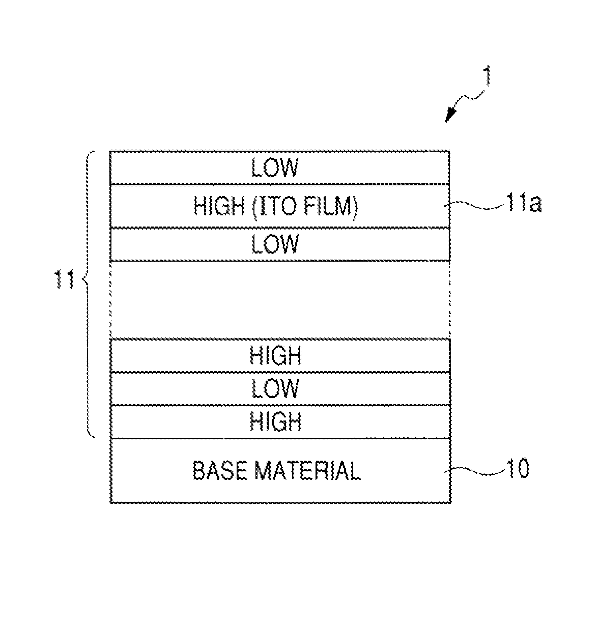
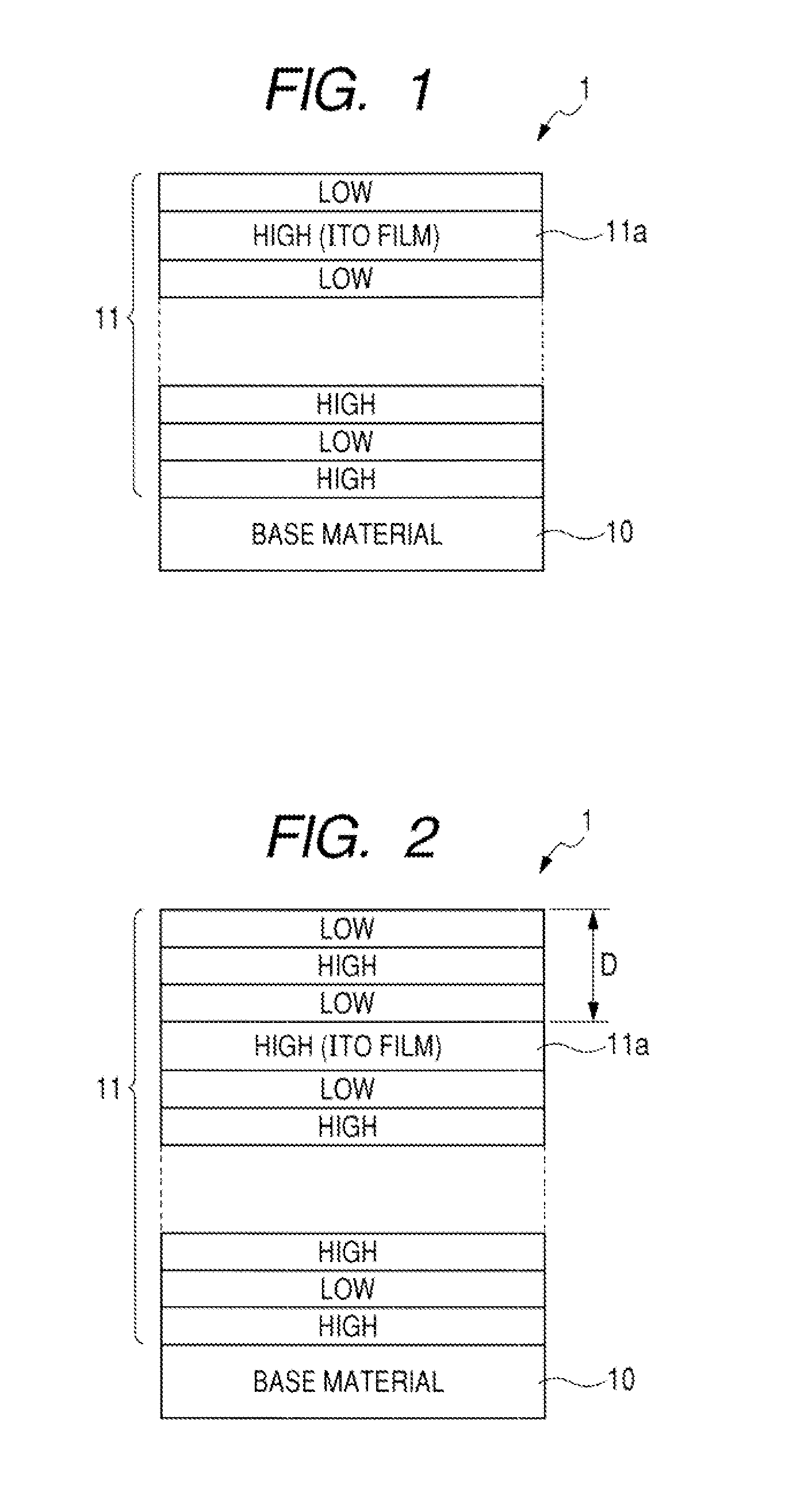
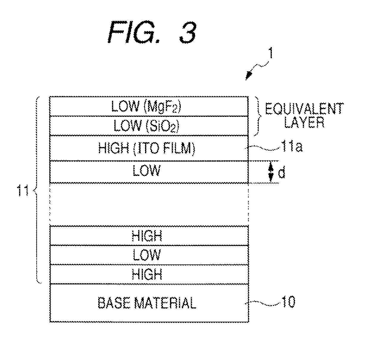
[0042]FIG. 1 is a schematic diagram showing an embodiment of a low-pass filter in the invention. A low-pass filter 1 in the drawing includes a coating layer 11 of blocking infrared radiation formed on the surface of a base material 10. The coating layer 11 of blocking the infrared radiation includes a high-refractive layer and a low-refractive layer sequentially disposed alternately on one on the other. One of the high-refractive layers is configured by an ITO (Indium Tin Oxide) film 11a made of a mixture of indium oxide and tin oxide being a transparent conductive material. With such a configuration, the surface of the coating layer is increased in conductivity, and the attachment of dirt and dust due to static buildup can be effectively prevented.

[0043]Among the high-refractive layers configuring the...


PUM

PropertyMeasurementUnit
thicknessaaaaaaaaaa
thicknessaaaaaaaaaa
thicknessaaaaaaaaaa

Abstract

On the light-entering surface side of a base material 10, a coating layer 11 in which a high-refractive layer and a low-refractive layer are sequentially disposed alternately on one on the other is provided for blocking infrared radiation. One of the high-refractive layers is configured by an ITO film 11a so that the conductivity is increased on the surface of the coating layer. Herein, in view of preventing, to a further extent, the attachment of dirt and dust by providing the conductivity to the surface of the coating layer, it is desirable if the outermost high-refractive layer is made of a transparent conductive material. Moreover, it is desirable if the total layer thickness is 140 nm or smaller for the refractive layers formed outside of the high-refractive layer made of the transparent conductive material.

Description

TECHNICAL FIELD[0001]The present invention relates to an optical low-pass filter (hereinafter, sometimes referred to simply as “low-pass filter”) and, more specifically, to an optical low-pass filter provided with a coating layer effectively working for infrared blocking, antireflection, and others.BACKGROUND ART[0002]In recent years, an imaging apparatus such as still video camera or video camera is becoming rapidly popular for electronically storing images. With such an imaging apparatus, the image of an object formed by a camera lens is converted into an electric signal for every pixel by an imaging device such as CCD and CMOS, and the result is stored in a recoding medium as image data.[0003]With such an imaging apparatus, because the imaging device includes regularly-aligned pixels on a light reception surface, when an object for imaging has any spatial frequency component approximated to a sampling spatial frequency that is determined by pixel spacing, moiré appears in the ima...

Claims


Application Information

Patent Timeline
Patent Type & Authority Patents(United States)
IPC IPC(8): G02B1/10G02B5/28G02B27/46H04N5/225H04N5/335
CPCG02B27/0006G02B27/46G03B19/12H04N5/23212H04N23/52H04N23/672H04N23/631G02B5/26G02B1/11
Inventor TSUJIMURA, ICHIRONOSE, MASAAKITANAKA, YOSHIHARUKUBO, NAOKI
Owner SONY CORP
Why Eureka
Try Eureka