
Method for forming metal oxides and silicides in a memory device

a memory device and metal oxide technology, applied in the field of memory devices, can solve the problems of insufficient resistance of low resistance metal oxide films to be used within a practical nonvolatile memory device, the inability to form reliable nonvolatile memory devices, and the inability to meet the requirements of low resistance metal oxide films

Active Publication Date: 2013-06-18
INTERMOLECULAR +2
View PDF3 Cites 23 Cited by
  • Summary
  • Abstract
  • Description
  • Claims
  • Application Information

AI Technical Summary

Benefits of technology

The patent describes methods for manufacturing nonvolatile memory devices using metal oxides and silicon materials. These methods allow for the use of wider ranges of metal oxides than previous techniques and can provide better switching properties. The methods also involve depositing a metallic layer and then oxidizing it to form a metal oxide layer containing a resistive switching metal oxide. The resulting memory devices have improved switching voltage and on / off currents. The methods also allow for the doping of the film stacks to meet specific requirements. The use of activated oxygen sources and the exposure of the substrate to ultraviolet sources can further enhance the quality of the memory devices.

Problems solved by technology

However, as device dimensions shrink, scaling issues are posing challenges for traditional nonvolatile memory technology.
Although metal oxide films such as these exhibit bistability, the resistance of these films and the ratio of the high-to-low resistance states are often insufficient to be of use within a practical nonvolatile memory device.
Therefore, a low resistance metal oxide film may not form a reliable nonvolatile memory device.
For example, in a nonvolatile memory that has conductive lines formed of a relatively high resistance metal such as tungsten, the resistance of the conductive lines may overwhelm the resistance of the metal oxide resistive switching element.
Therefore, the state of the bistable metal oxide resistive switching element may be difficult or impossible to sense.
Similar issues can arise from integration of the resistive switching memory element / device with current steering elements, such as diodes and / or resistors.
However, since the power that can be delivered to a circuit containing a series of resistive switching memory elements and current steering elements is typically limited in most conventional nonvolatile memory devices (e.g., CMOS driven devices), it is desirable to form each of the resistive switching memory elements and current steering elements in the circuit so that the voltage drop across each of these elements is small, and thus resistance of the series connected elements does not cause the current to decrease to an undesirable level due to the fixed applied voltage (e.g., about 2-5 volts).
Metallic silicide materials may be deposited by sputtering from a composite target, however, control of the stoichiometry of the metallic silicide is often difficult and unsuccessful.
In examples of metal oxide films used in bipolar switching devices, the metal oxide must remain free of metallic ion impurities or else the degraded metal oxide becomes unreliable and the overall device will fail.
The switching effect of the memory device generally occurs due to anionic defects, such as oxygen vacancies, within the metal oxide films.
However, if a metallic silicide layer is in contact with an adjacent switching metal oxide film, a portion of the metal within the metallic silicide material will likely diffuse into the switching metal oxide film and greatly degrade the reliability of the switching effect.

Method used


Image

  • Method for forming metal oxides and silicides in a memory device
  • Method for forming metal oxides and silicides in a memory device
  • Method for forming metal oxides and silicides in a memory device

Examples


Embodiment Construction

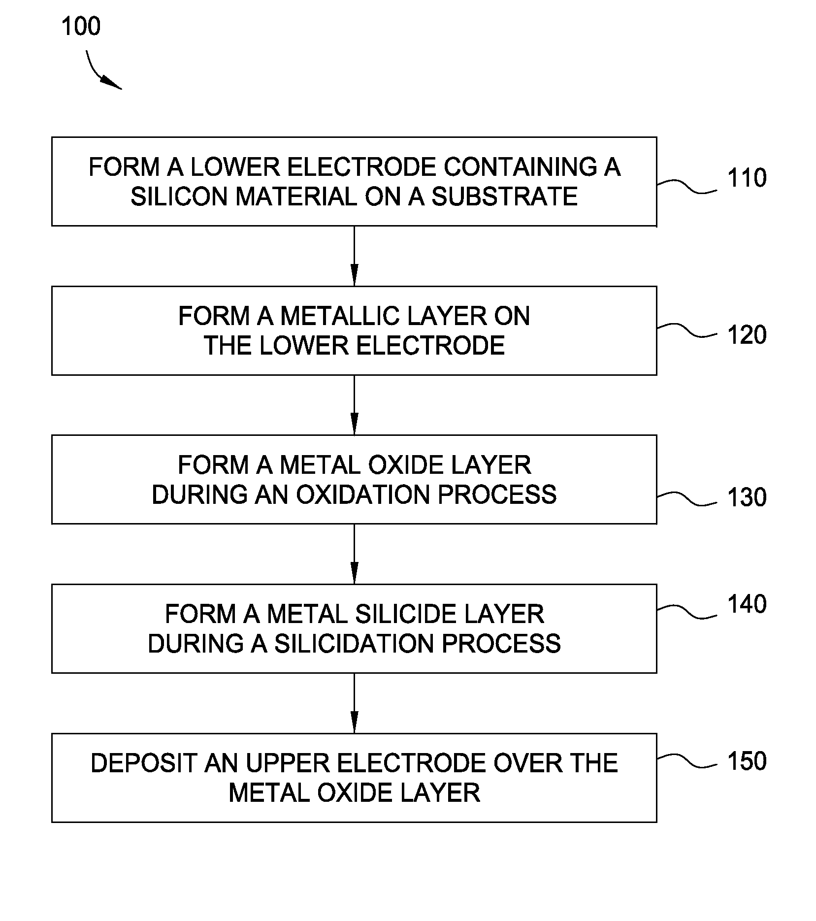
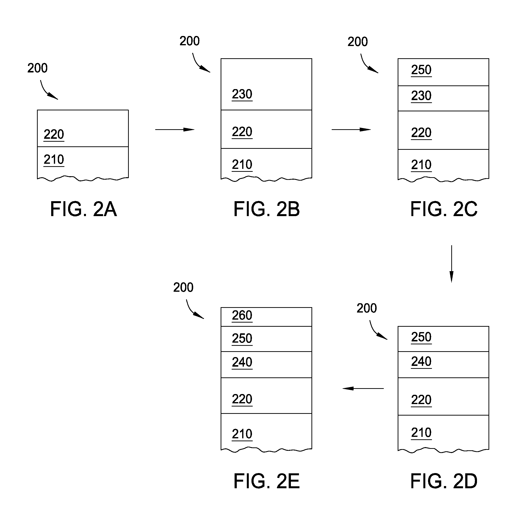
[0026]Embodiments of the invention generally relate to nonvolatile memory devices and methods for manufacturing such memory devices. The methods described herein provide a broader range of metal oxides and metal silicides than available with previous deposition techniques. The metal silicide materials in some examples provide a better interface for the lower electrode by reducing switching voltage and on / off currents relative to pure silicon. The methods provide desired doping of the metal oxide / silicide film stack by utilizing the specified temperatures during the oxide / silicide formation processes, therefore, metal oxide / silicide film stacks may be formed which meet or exceed the requirements of switching voltage and on / off currents.

[0027]FIG. 1 is a flowchart illustrating a method for manufacturing or otherwise forming various memory devices, as described by embodiments herein, such as process 100 which may be utilized to form resistive switching memory elements / devices, such as ...


PUM

PropertyMeasurementUnit
temperatureaaaaaaaaaa

Abstract

Embodiments of the invention generally relate to memory devices and methods for fabricating such memory devices. In one embodiment, a method for fabricating a resistive switching memory device includes depositing a metallic layer on a lower electrode disposed on a substrate and exposing the metallic layer to an activated oxygen source while heating the substrate to an oxidizing temperature within a range from about 300° C. to about 600° C. and forming a metal oxide layer from an upper portion of the metallic layer during an oxidation process. The lower electrode contains a silicon material and the metallic layer contains hafnium or zirconium. Subsequent to the oxidation process, the method further includes heating the substrate to an annealing temperature within a range from greater than 600° C. to about 850° C. while forming a metal silicide layer from a lower portion of the metallic layer during a silicidation process.

Description

BACKGROUND OF THE INVENTION[0001]1. Field of the Invention[0002]Embodiments of the invention generally relate to memory devices and methods for manufacturing such memory devices.[0003]2. Description of the Related Art[0004]Nonvolatile memory elements are used in systems in which persistent storage is required. For example, digital cameras use nonvolatile memory cards to store images and digital music players use nonvolatile memory to store audio data. Nonvolatile memory is also used to persistently store data in computer environments. Nonvolatile memory is often formed using electrically-erasable programmable read only memory (EPROM) technology. This type of nonvolatile memory contains floating gate transistors that can be selectively programmed or erased by application of suitable voltages to their terminals.[0005]As fabrication techniques improve, it is becoming possible to fabricate nonvolatile memory elements with increasingly smaller dimensions. However, as device dimensions sh...

Claims


Application Information

Patent Timeline
Patent Type & Authority Patents(United States)
IPC IPC(8): H01L21/00H01L21/16H01L21/332H10B99/00
CPCH01L27/101H01L45/08H01L45/1233H01L45/146H01L45/16H01L45/1608H01L45/1253H01L27/2463H10B63/80H10N70/24H10N70/826H10N70/841H10N70/8833H10N70/021H10N70/011
Inventor PRAMANIK, DIPANKARCHIANG, TONY P.MINVIELLE, TIMYAMAGUCHI, TAKESHI
Owner INTERMOLECULAR
Learn More