Receiving circuit, LSI chip, and storage medium

a technology of receiving circuit and storage medium, applied in the field of receiving circuit, can solve problems such as difficulty in reducing circuit scale and circuit siz

Inactive Publication Date: 2013-06-18
SEMICON ENERGY LAB CO LTD
View PDF122 Cites 13 Cited by
  • Summary
  • Abstract
  • Description
  • Claims
  • Application Information

AI Technical Summary

Benefits of technology

[0007]Such a technique of wireless communication utilizing electromagnetic induction can be applied to a small IC chip, a storage medium such as a flash memory, or the like. By application of this technique to the storage medium or the like, an area can be markedly reduced by elimination of an exposed portion of a contact electrode that has been needed; thus, further reduction in the size of the storage medium is expected. In addition, since the exposed electrode is not needed, the IC chip or the storage medium can be covered with resin or the like and be totally waterproof Further, a slot into which a storage medium is inserted can be eliminated from an electronic device. In the above manner, advantageous effects are expected in various aspects.
[0008]Here, the structure and operation of the conventional receiving circuit used for wireless communication utilizing electromagnetic induction are described with reference to FIG. 10 and FIGS. 11A to 11C. FIG. 10 is a circuit diagram illustrating a structure example of part of a transmitting circuit and the conventional receiving circuit.
[0009]FIGS. 11A to 11C are examples of timing charts at the time when signals are transmitted and received.
[0010]A transmitting circuit 10 includes a coil 11. One terminal of the coil 11 is connected to a ground potential line, and a transmitting signal TXDATA is input from the other terminal of the coil 11. A receiving circuit 20 includes a coil 21, two comparators (a comparator 23a and a comparator 23b), and a latch circuit 25 including NAND circuit elements. One terminal of the coil 21 is connected to a ground potential line, and the other terminal of the coil 21 is connected to an inversion input terminal (hereinafter also referred to as a−terminal (a minus terminal)) of the comparator 23a and a non-inversion input terminal (hereinafter also referred to as a+terminal (a plus terminal)) of the comparator 23b.Reference voltage VH and reference voltage VL are input to a+terminal of the comparator 23a and a−terminal of the comparator 23b, respectively. Voltage which is higher than 0 V and voltage which is lower than 0 V are used as the reference voltage VH and the reference voltage VL, respectively. Output terminals of the comparators 23a and 23b are connected to the latch circuit 25, and a receiving signal RXDATA is output from the latch circuit 25.
[0011]Here, in order to clearly show the relative position of the two coils of the transmitting circuit 10 and the receiving circuit 20, black circles are shown at one ends of the coils in FIG. 10. Specifically, in the case where a coupling factor is positive, it is assumed that the direction of current with respect to one end of the coil on a primary side at which the black circle is shown is the same as the direction of current with respect to one end of the coil on a secondary side at which the black circle is shown. Note that in this structure, a coupling factor between the two coils is assumed to be positive.
[0012]Next, reception operation is described with reference to FIG. 10 and timing charts in FIGS. 11A to 11C. FIG. 11A illustrates transition of the voltage of the transmitting signal TXDATA over time. FIG. 11B illustrates transition of a potential difference VR generated between both ends of the coil 21 over time. FIG. 11C illustrates transition of the voltage of the receiving signal RXDATA over time. Here, the level of VR is equal to the level of voltage input to the−terminal of the comparator 23a and the +terminal of the comparator 23b under the condition that the direction of the one end of the coil 21 in FIG. 10 at which the black circle is shown is positive.

Problems solved by technology

In this manner, not only the conventional receiving circuit with the above structure but also another conventional receiving circuit has large circuit scale, and it is difficult to reduce the circuit scale and circuit size and to highly integrate the circuit.

Method used


Image

  • Receiving circuit, LSI chip, and storage medium
  • Receiving circuit, LSI chip, and storage medium
  • Receiving circuit, LSI chip, and storage medium

Examples


embodiment 1

(Embodiment 1)

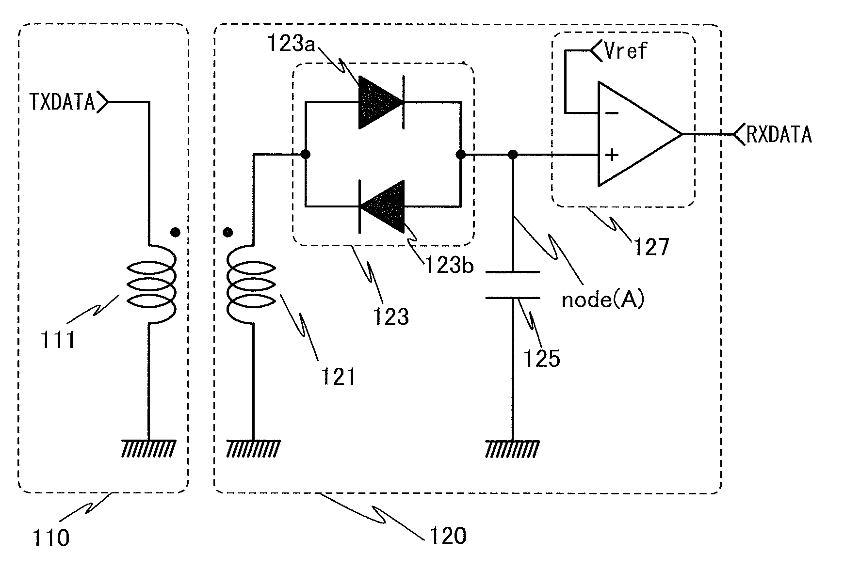
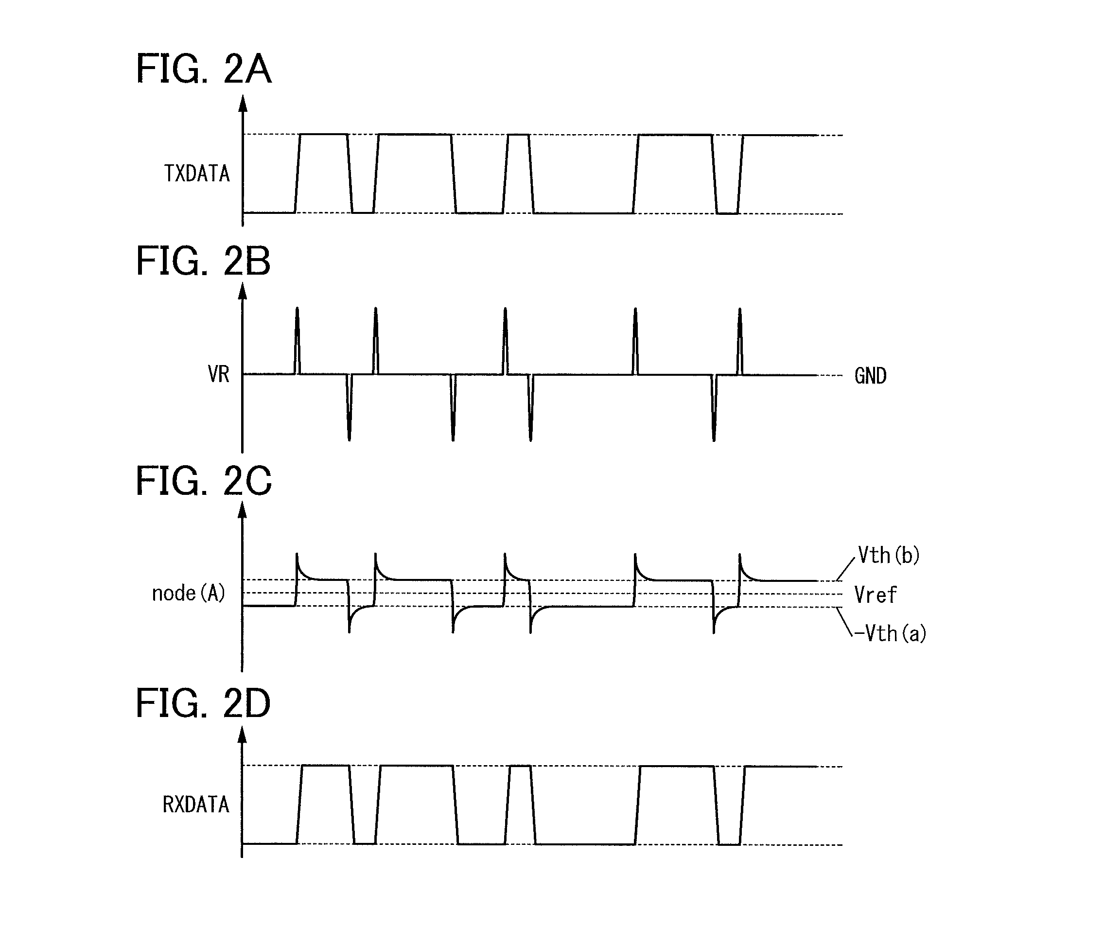
[0049]In this embodiment, a receiving circuit in one embodiment of the present invention is described with reference to FIG. 1 and FIGS. 2A to 2D. FIG. 1 is a circuit diagram illustrating a structure example of part of a transmitting circuit and a receiving circuit in this embodiment. FIGS. 2A to 2D are examples of timing charts at the time when signals are transmitted and received.

[0050]First, circuit structures of a transmitting circuit 110 and a receiving circuit 120 in this embodiment are described with reference to FIG. 1.

[0051]The transmitting circuit 110 has a function of transmitting a transmitting signal with the use of a coil. The transmitting circuit 110 in this embodiment includes a coil 111. One terminal of the coil 111 is connected to a ground potential line, and a transmitting signal TXDATA is input to the other terminal of the coil 111. Note that although the one terminal of the coil 111 is grounded in this embodiment, this embodiment is not limited to ...

embodiment 2

(Embodiment 2)

[0074]In this embodiment, a structure where a transistor whose leakage current is markedly reduced is used as the diode element in the receiving circuit in Embodiment 1 is described with reference to FIG. 3, FIG. 4, and FIGS. 5A to 5D.

[0075]FIG. 3 illustrates structure examples of the transmitting circuit 110 and a receiving circuit 220 in this embodiment.

[0076]The transmitting circuit 110 has the same structure as that in Embodiment 1. The receiving circuit 220 has a structure which is similar to that of the receiving circuit 120 in Embodiment 1 except that the diode element 123a and the diode element 123b in the parallel circuit 123 are replaced with a transistor 223a and a transistor 223b, respectively. In other words, a coil 221, a capacitor 225, and a comparison circuit 227 are similar to the coil 121, the capacitor 125, and the comparison circuit 227 in the receiving circuit 120, respectively.

[0077]A parallel circuit 223 includes the transistor 223a and the trans...

embodiment 3

(Embodiment 3)

[0103]In this embodiment, an example of an LSI chip including a receiving circuit in one embodiment of the present invention is described with reference to FIG. 6.

[0104]FIG. 6 is a schematic diagram illustrating the structures of three LSI chips which are stacked and signal transmission and reception in the three LSI chips. LSI chips 301 to 303 illustrated in FIG. 6 each include a plurality of receiving circuits and a plurality of transmitting circuits. Arrows in FIG. 6 show the directions of signals transmitted from the transmitting circuit to the receiving circuit.

[0105]Signals are transmitted and received between a set of transmitting and receiving circuits in each LSI chip. Thus, in the case where the LSI chips are stacked, it is preferable that coils of the set of transmitting and receiving circuits substantially overlap with each other because a coupling factor between the coils can be increased. The size and shape of the coils of the transmitting and receiving c...


PUM


Abstract

A receiving circuit with a simple circuit structure for performing wireless communication utilizing electromagnetic induction is provided. An LSI chip and a storage medium where wireless communication utilizing electromagnetic induction is performed and the circuit scale and circuit size can be reduced are provided. The following receiving circuit may be used: a parallel circuit where two diode elements whose directions are opposite are connected in parallel is used, one end of the parallel circuit is connected to the other end of a coil whose one end is connected to a ground potential line, and a capacitor is connected in series with the other end of the parallel circuit. A transistor whose leakage current is markedly reduced may be used as a diode in the receiving circuit. Such a receiving circuit may be used in an LSI chip or a storage medium.

Description

BACKGROUND OF THE INVENTION[0001]1. Field of the Invention[0002]The present invention relates to receiving circuits used for wireless communication utilizing electromagnetic induction. The present invention relates to LSI (semiconductor integrated circuit) chips capable of performing wireless communication utilizing electromagnetic induction. The present invention relates to storage media capable of performing wireless communication utilizing electromagnetic induction.[0003]2. Description of the Related Art[0004]An electronic circuit for performing wireless communication utilizing electromagnetic induction by a combination of a semiconductor element such as an LSI chip and a coil has been proposed (Reference 1). For example, the electronic circuit disclosed in Reference 1 can perform communication between LSI chips or between an electronic device and an LSI chip and is expected to be applied to an LSI layering technology, an IC chip, or the like.[0005]For example, in the case where ...

Claims


Application Information

Patent Timeline
Patent Type & Authority Patents(United States)
IPC IPC(8): H01L29/93
CPCH04B5/0031H04B5/0081
Inventor KAMATA, KOICHIRO
Owner SEMICON ENERGY LAB CO LTD
Why Eureka
Try Eureka