Method for forming a multilayer structure

a multi-layer structure and etching method technology, applied in the field of forming multi-layer structures, can solve the problems of high selectivity, high etch rate and high selectivity of silicon-germanium etching methods, and unsuitable multi-layer structures for several devices, etc., to achieve the effect of removing quickly and selectively

Active Publication Date: 2013-06-25
COMMISSARIAT A LENERGIE ATOMIQUE ET AUX ENERGIES ALTERNATIVES +1
View PDF8 Cites 151 Cited by
  • Summary
  • Abstract
  • Description
  • Claims
  • Application Information

AI Technical Summary

Problems solved by technology

However, the Si / SiGe multilayer structure is unsuitable for formation of several devices, in particular Micro-Electro-Mechanical Systems (MEMS), due to certain dimensional constraints.
Firstly, silicon-germanium etching methods do not allow both a high etch rate and a high selectivity with respect to silicon.
This results in over-etching of the silicon layers and / or a limitation on the length of the SiGe layers.
Secondly, the thickness of the SiGe layers is limited, as is the number of periods in the structure.
It is therefore not possible to increase the germanium concentration to increase the etch rate or selectivity.

Method used


Image

  • Method for forming a multilayer structure
  • Method for forming a multilayer structure
  • Method for forming a multilayer structure

Examples


Embodiment Construction

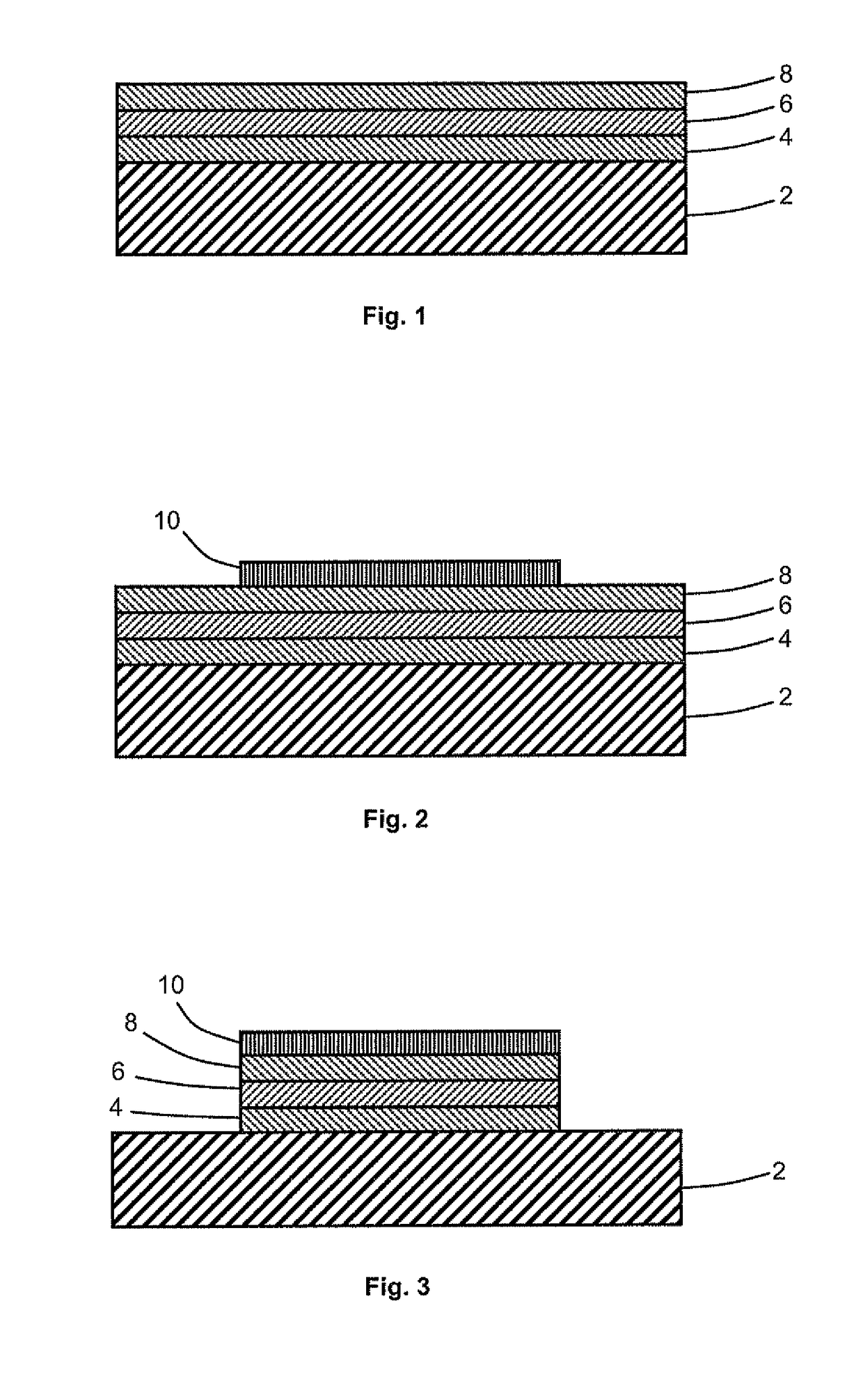
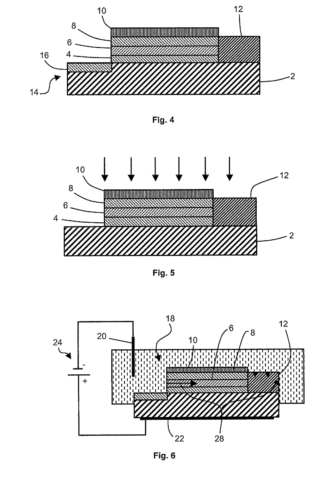
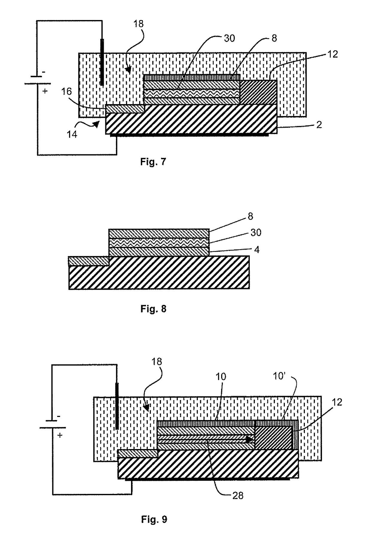
[0020]It is envisaged to form a multilayer structure comprising at least one bulk silicon layer and one porous silicon layer. Unlike silicon-germanium, porous silicon can be etched quickly and with great selectivity with respect to bulk silicon.

[0021]Porous silicon is generally obtained by anodic dissolution, also called anodization, of a sample of bulk silicon in a hydrofluoric acid (HF) based-electrolyte. The silicon sample is placed in an electrochemical bath having a hydrofluoric acid concentration comprised between about 1% and 50%. An electric field is applied by placing a first electrode (cathode) in the electrolyte and a second electrode (anode) in electric contact with the sample. This contact can be direct by applying the electrode on the sample, or indirect, for example via an electrolyte. In certain cases, the sample is exposed to light radiation to enable the dissolution reaction.

[0022]Anodization of the silicon results from an equilibrium between mass transport in the ...


PUM

PropertyMeasurementUnit
porosityaaaaaaaaaa
porosityaaaaaaaaaa
thicknessaaaaaaaaaa

Abstract

The method for forming a multilayer structure on a substrate comprises providing a stack successively comprising an electron hole blocking layer, a first layer made from N-doped semiconductor material having a dopant concentration greater than or equal to 1018 atoms / cm3 or P-doped semiconductor material, and a second layer made from semiconductor material of different nature. A lateral electric contact pad is made between the first layer and the substrate, and the material of the first layer is subjected to anodic treatment in an electrolyte.

Description

BACKGROUND OF THE INVENTION[0001]The invention relates to a method for forming a multilayer structure on a substrate, and more particularly to a method for forming an alternation of bulk silicon layers and porous silicon layers.STATE OF THE ART[0002]Substrates comprising an alternation of layers of semiconductor materials enable formation of advanced microelectronic devices. The article “Novel 3D integration process for highly scalable Nano-Beam stacked-channels GAA (NBG) FinFETs with HfO2 / TiN gate stack” (Ernst. T et al., Electron Devices Meeting, 2006, IEDM '06. International, pp. 1-4) describes for example formation of a multichannel transistor from a silicon / silicon-germanium multilayer structure.[0003]This structure is obtained by successive epitaxies of silicon (Si) layers and of silicon-germanium (SiGe) layers. When growth of a SiGe layer takes place on a Si layer, the lattice parameter of the silicon-germanium adapts to the lattice parameter of the silicon. The epitaxied sil...

Claims


Application Information

Patent Timeline
Patent Type & Authority Patents(United States)
IPC IPC(8): H01L21/30
CPCB81C1/0038H01L21/306B81C2201/0109B81C2201/0115
Inventor DESPLOBAIN, SEBASTIENGAILLARD, FREDERIC-XAVIERMORAND, YVESNEMOUCHI, FABRICE
Owner COMMISSARIAT A LENERGIE ATOMIQUE ET AUX ENERGIES ALTERNATIVES
Why Eureka
Try Eureka