Method for thinning a bonding wafer

a bonding wafer and thinning technology, applied in the field of semiconductor/solid-state device manufacturing, can solve the problems of subsurface damage on the prime surface of the wafer, unsupported area beyond the bonding layer becoming problematic, and the top wafer thinned down to microns of thickness

Active Publication Date: 2013-07-02
TOKYO ELECTRON LTD
View PDF12 Cites 102 Cited by
  • Summary
  • Abstract
  • Description
  • Claims
  • Application Information

AI Technical Summary

Problems solved by technology

In cases where the bonding layer does not extend to the outer diameter, the top wafer is thinned down to microns of thickness and the unsupported area beyond the bonding layer becomes problematic.
The thinning process tends to chip the unsupported wafer edge and the debris created causes scratching and subsurface damage on the prime surface of the wafer.
Furthermore, in the chase of wafer thinning processes that utilize wet etching, exposed areas of the bonding layer may be chemically etched or attacked by the wet etching chemicals, thereby compromising the structural integrity of a device containing the top wafer and possibly lead to a loss of yield.
A more extreme example of the damage is that large pieces of the top wafer break off with the bonding layer attached.
However, this technique is costly and adds long cycle times to the processing.
However, the side of the top wafer is not protected and mechanical damage can occur during subsequent planarization and thinning of the top wafer and the bonding layer may be damaged.
In the case of wet etching processes, a chemical attack on the bonding layer can create mechanical instability of the device and increase the probability of damage.
Furthermore, trapped chemical species on the bonded side of the top wafer can diffuse to other areas of the top wafer and degrade or destroy the device.

Method used


Image

  • Method for thinning a bonding wafer
  • Method for thinning a bonding wafer
  • Method for thinning a bonding wafer

Examples


Embodiment Construction

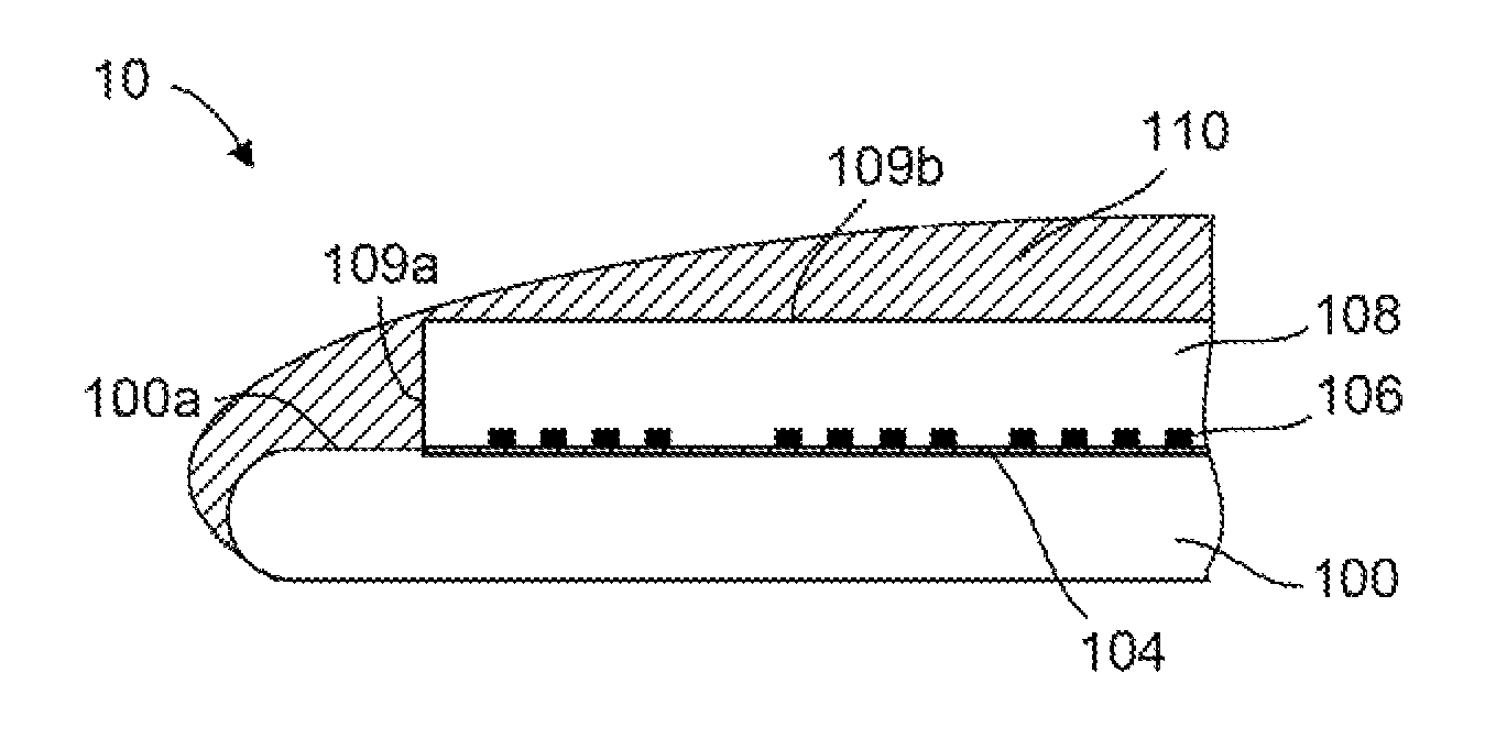
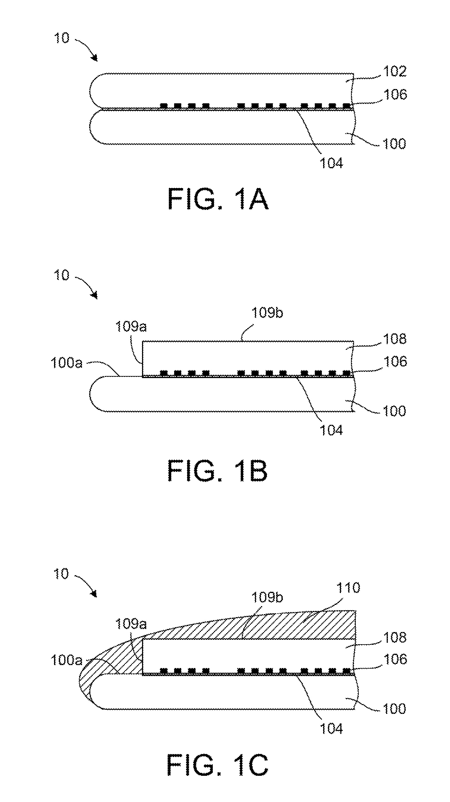
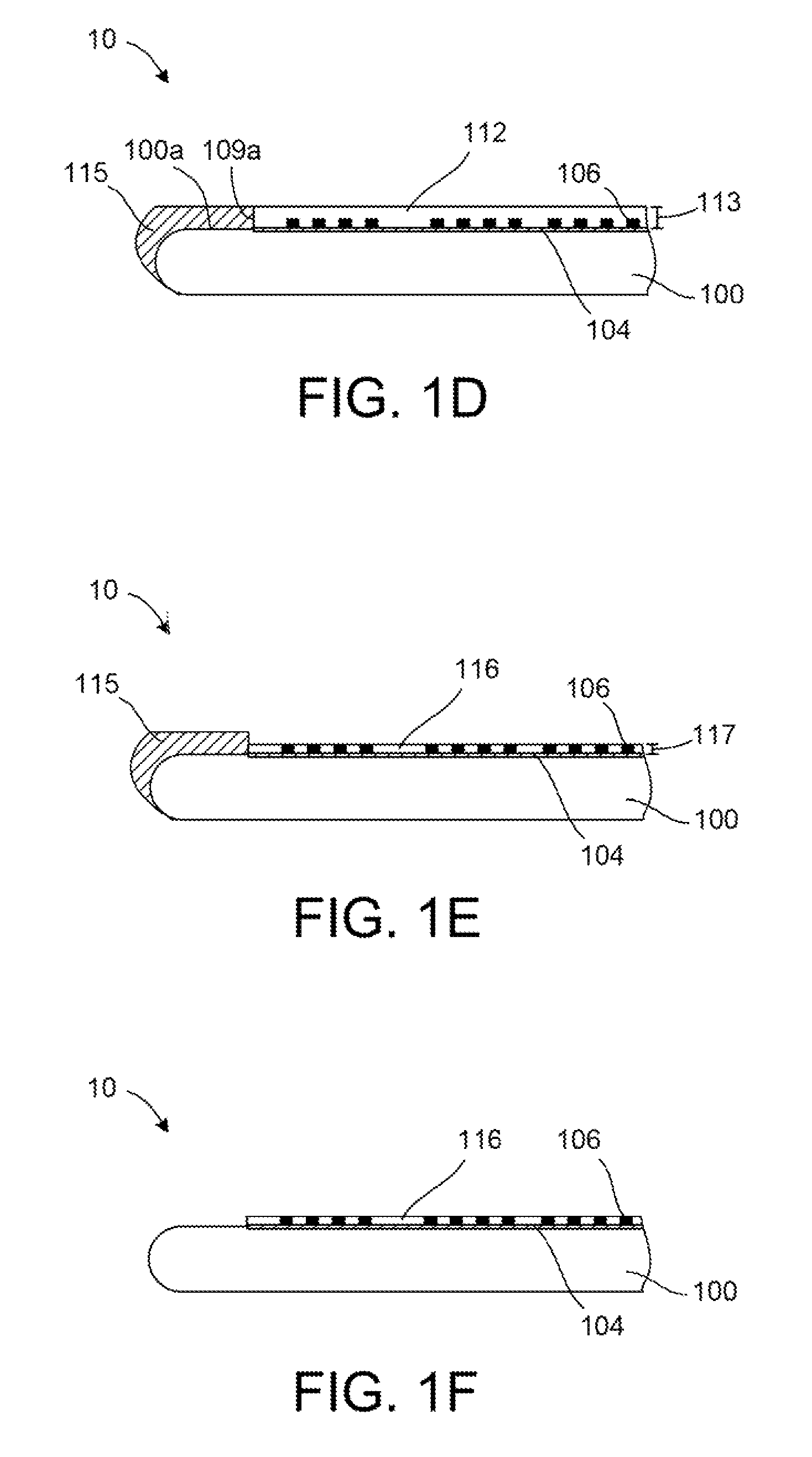
[0013]Methods for thinning wafers, for example wafers containing Through Silicon Vias (TSV), are disclosed in various embodiments.

[0014]FIG. 1A schematically shows a structure 10 containing a handling wafer 100 coupled to a silicon bonding wafer 102 using a bonding layer 104. The handling wafer 100 and the silicon bonding wafer 102 may be silicon wafers having a radius of 100 mm, 150 mm, 225 mm, or larger. Furthermore, the handling wafer 100 and the silicon bonding wafer 102 may each have total thickness of approximately 1 mm. The silicon bonding wafer 102 further contains a plurality of metal filled vias (holes) 106 in contact with the bonding layer 104. The metal filled vias 106 can, for example, have a diameter between about 1 micron (micron=10−6 meter) and about 50 microns, for example about 25 microns or about 40 microns. In one example, the metal filled vias 106 may have a diameter of about 25 microns and a height of about 25 microns. In some examples, the metal filled vias 10...


PUM


Abstract

A method is provided for thinning a wafer, for example a wafer containing Through Silicon Vias (TSV). The method includes providing a bonding wafer coupled to a handling wafer, and performing a wafer edge trimming process that forms a trimmed bonding wafer, where the wafer edge trimming process removes an edge portion of the bonding wafer and exposes an upper surface of the handling wafer. The method further includes forming a protective mask on the trimmed bonding wafer and on the exposed upper surface of the handling wafer, planarizing the protective mask and the trimmed bonding wafer, and selectively removing the planarized protective mask by an etching process. In one embodiment, the removing includes performing a first wet etching process that selectively removes a portion of the planarized trimmed bonding wafer relative to the planarized protective mask, and performing a second wet etching process that selectively removes the planarized protective mask.

Description

CROSS REFERENCE TO RELATED APPLICATION[0001]This application claims priority to U.S. provisional application Ser. No. 61 / 165,898, filed on Apr. 1, 2009, the entire contents of which are herein incorporated by reference.FIELD OF INVENTION[0002]The present invention relates to the field of semiconductor manufacturing, and more particularly, to methods for thinning a bonded wafer, for example a wafer containing Through Silicon Vias (TSV).BACKGROUND OF THE INVENTION[0003]As is known, wafers for the semiconductor industry have been bonded together by a bonding layer in a sandwich type relation for various applications. Further, for these applications, the top wafer diameter needs to be reduced while the diameter of the bottom or handling wafer remains unchanged. In cases where the bonding layer does not extend to the outer diameter, the top wafer is thinned down to microns of thickness and the unsupported area beyond the bonding layer becomes problematic. The thinning process tends to ch...

Claims


Application Information

Patent Timeline
Patent Type & Authority Patents(United States)
IPC IPC(8): H01L21/302
CPCH01L21/304H01L21/30608H01L21/30625
Inventor TRICKETT, DOUGLAS MYAMASHITA, ATSUSHI
Owner TOKYO ELECTRON LTD
Why Eureka
Try Eureka