Injection molded solder process for forming solder bumps on substrates

a technology of injection molding and substrate, which is applied in the direction of non-electric welding apparatus, manufacturing tools, and soldering apparatus, etc., can solve the problems of non-uniform height of pillars and caps, compromising the ability to ensure reliable interconnection, and not revealing the formation of bumps of uniform height on non-uniform copper pillars. to achieve the effect of minimizing or eliminating the spillage of solder

Inactive Publication Date: 2013-07-30
INT BUSINESS MASCH CORP
View PDF20 Cites 3 Cited by
  • Summary
  • Abstract
  • Description
  • Claims
  • Application Information

AI Technical Summary

Benefits of technology

[0008]An assembly is provided in accordance with a further aspect of the invention for injecting solder on round wafers evenly and while minimizing or eliminating spillage of solder. Such an assembly comprises a carrier including a circular recess and a planar surface surrounding the circular recess, the diameter of the recess being smaller than the length and width of the carrier. A fill head is provided for depositing molten solder positioned over the carrier and engaging the planar surface of the carrier, the fill head including a slot for dispensing solder, the length of the slot being substantially the same as the diameter of the circular recess.

Problems solved by technology

The copper pillars and solder caps may each be formed by electroplating, which process can lead to non-uniformity in the heights of the pillars and caps.
There may accordingly be more or less solder in the pillar-cap assemblies, compromising the ability to ensure reliable interconnections following reflow.
This method also does not disclose forming bumps of uniform height on non-uniform copper pillars.

Method used


Image

  • Injection molded solder process for forming solder bumps on substrates
  • Injection molded solder process for forming solder bumps on substrates
  • Injection molded solder process for forming solder bumps on substrates

Examples


Embodiment Construction

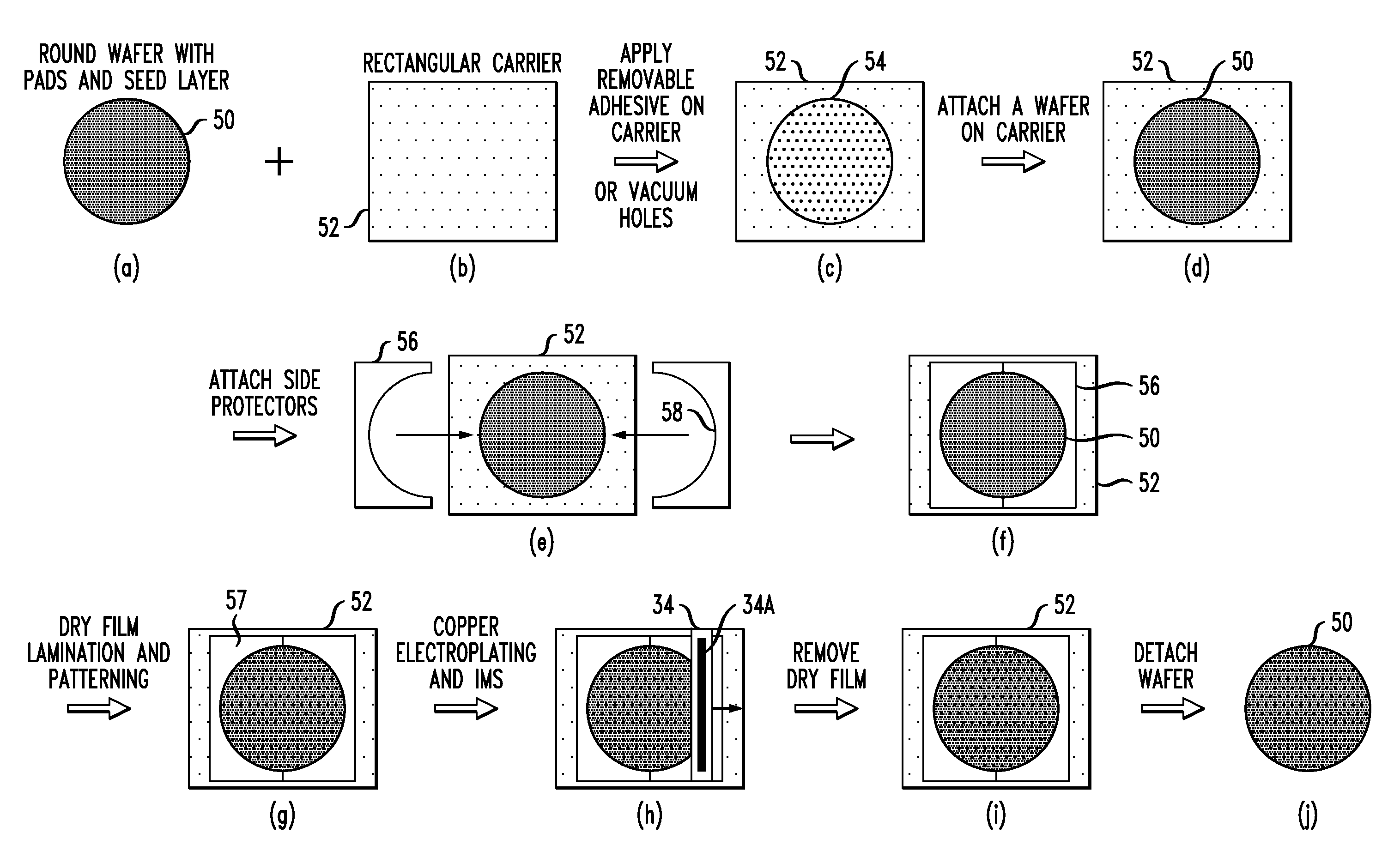
[0017]Initially, the complete disclosure of commonly assigned U.S. patent application Ser. No. 12 / 706,212 filed Feb. 16, 2010, entitled “Direct IMS (Injection Molded Solder) Without a Mask for Forming Solder Bumps on Substrates” and U.S. Pub. No. 2010 / 0116871 entitled “Injection Molded Solder Method for Forming Solder Bumps on Substrates” are expressly incorporated herein by reference in their entireties for all purposes.

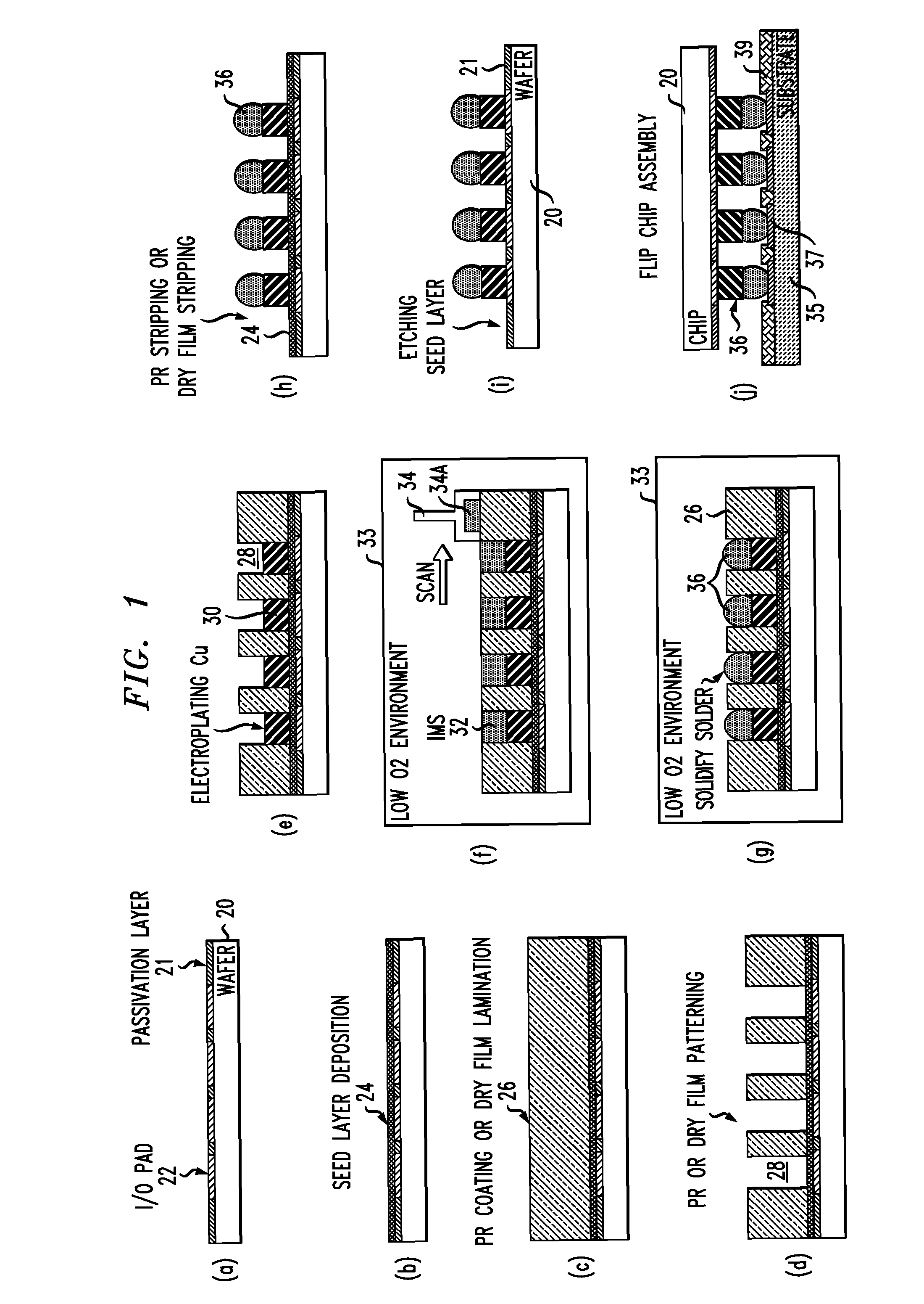
[0018]Referring to FIGS. 1(a)-1(j), steps in performing a method in accordance with one aspect of the invention are shown. A wafer 20 including a passivation layer 21 and rows of I / O pads 22 is shown in FIG. 1(a). The wafer may be comprised of silicon or other suitable composition. The pads 22 are made from a conductive material such as copper or aluminum. A thin, conductive seed layer 24 is deposited on the wafer as shown in FIG. 1(b). The seed layer is comprised of a suitable metal(s) such as TiCu. A photoresist layer 26 is applied to the seed layer as shown in FI...


PUM

PropertyMeasurementUnit
thicknessaaaaaaaaaa
thicknessaaaaaaaaaa
heightaaaaaaaaaa

Abstract

Solder bumps of uniform height are provided on a substrate through the use of injection molded solder. Copper pillars or ball limiting metallurgy are formed over I / O pads within the channels of a patterned layer of photoresist. Solder is injected over the pillars or BLM, filling the channels. The solder, which does not contain flux, is allowed to solidify. It forms a plurality of solder structures (bumps) of equal heights. Solder injection and solidification are preferably carried out in a nitrogen environment or a forming gas environment. Molten solder can be injected in channels formed in round wafers without spillage using a carrier assembly that accommodates such wafers and a fill head.

Description

FIELD OF THE INVENTION[0001]The present invention generally relates to the electrical and electronic arts and, more particularly, to injection molded solder techniques, and solder deposition on substrates.BACKGROUND OF THE INVENTION[0002]Flip chip technology has been widely used as it allows a high I / O count, high density interconnection scheme with proven performance and reliability. Solder bumps are deposited on contact pads on chip surfaces and the chips are then flipped and positioned such that the solder bumps are aligned with matching pads of an external circuit. Solder reflow completes the interconnection process, after which underfill material is introduced to fill the spaces about the interconnections.[0003]Flip chip interconnection assemblies have included copper pillars having solder caps. The copper pillars and solder caps may each be formed by electroplating, which process can lead to non-uniformity in the heights of the pillars and caps. There may accordingly be more o...

Claims


Application Information

Patent Timeline
Patent Type & Authority Patents(United States)
IPC IPC(8): B23K3/00B23K3/06
CPCB23K1/0016B23K3/0623H01L24/11H01L24/13H01L21/6835B23K1/20H01L2924/00014B23K2201/42H01L24/03H01L24/05H01L2221/68372H01L2224/03464H01L2224/0401H01L2224/05571H01L2224/05573H01L2224/05624H01L2224/05644H01L2224/05647H01L2224/05655H01L2224/05664H01L2224/11312H01L2224/11462H01L2224/1147H01L2224/11849H01L2224/11902H01L2224/13082H01L2224/13111H01L2224/13144H01L2224/13147H01L2224/13155H01L2224/13164H01L2224/16237H01L2224/94H01L2224/11002H01L2924/01322H01L2224/03H01L2224/11H01L2924/00012H01L2924/01029H01L2924/01047H01L2924/01083H01L2924/01049H01L2924/01079H01L2924/00H01L2224/05552H01L2924/00011H01L2224/1403H01L2224/14505B23K2101/42H01L2224/13023H01L2224/81805
Inventor FEGER, CLAUDIUSMCLEOD, MARK H.NAH, JAE-WOONGPERFECTO, ERIC D.
Owner INT BUSINESS MASCH CORP
Why Eureka
Try Eureka