

Preparation of nanoparticle materials
a nanoparticle and nanoparticle technology, applied in the field of nanoparticle materials, can solve the problems of particle agglomeration, low quantum efficiency, and difficult preparation of nanoparticles
- Summary
- Abstract
- Description
- Claims
- Application Information
AI Technical Summary
Benefits of technology
Problems solved by technology
Method used
Image

Examples
example 1
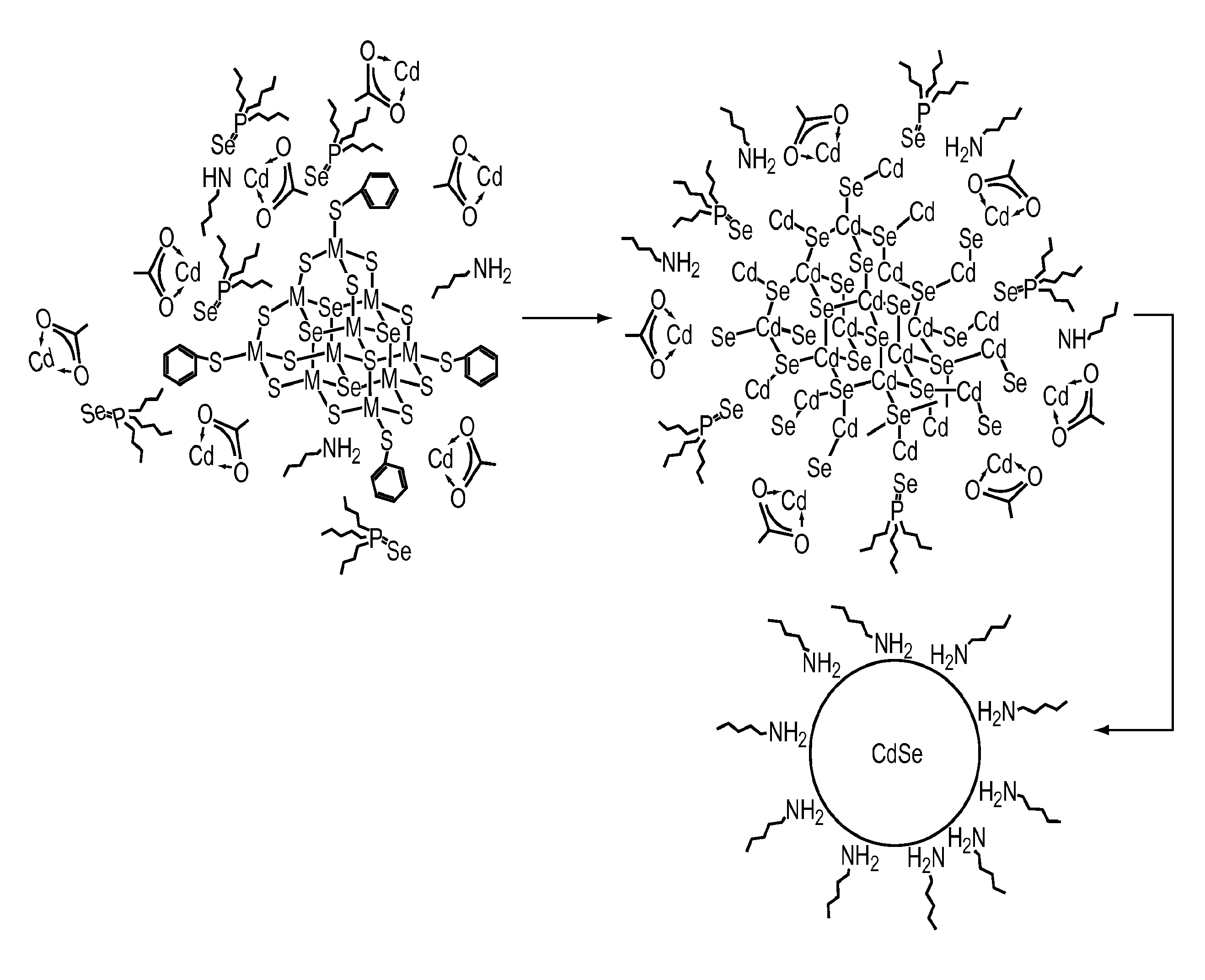
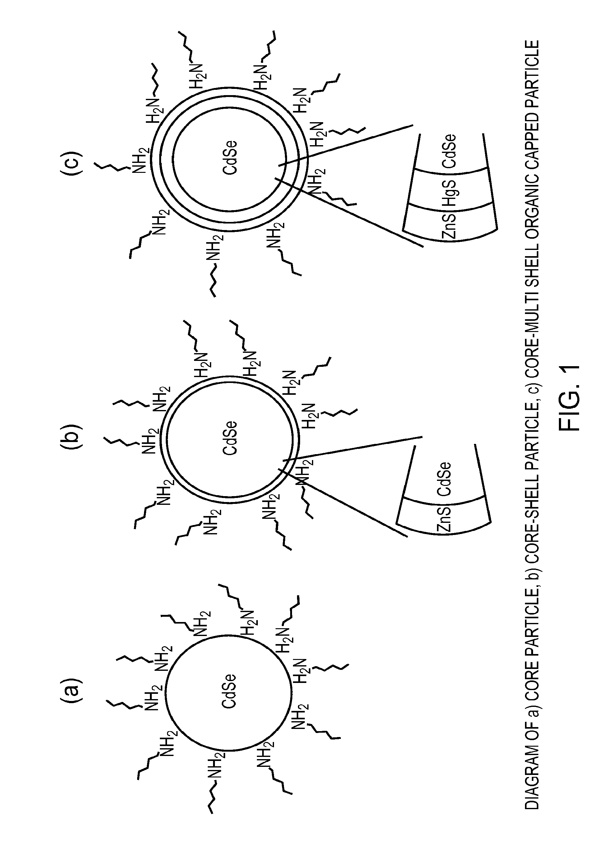
Preparation of CdSe Nanoparticles from [Et3NH]4[Cd10Se4(SPh)16] / TOPSe / Cd(CH3CO2)2 in HDA
[0108]HDA (300 g) was placed in a three-neck flask and dried / degassed by heating to 120° C. under a dynamic vacuum for 1 hour. The solution was then cooled to 70° C. To this was added 1.0 g of [Et3NH]4[Cd10Se4(SPh)16] (0.311 mmol), TOPSe (20 ml, 40.00 mmol) [previously prepared from dissolving selenium powder in TOP] and Cd(CH3CO2)2 (10.66 g 40.00 mmol) the temperature of reaction mixture was gradually increased from 70° C. to 180° C. over an 8 hour period. The progressive formation / growth of the nanoparticles was monitored by their emission wavelength by taking aliquots from the reaction mixture and measuring their UV-vis and PL spectra. The reaction was stopped when the emission spectra had reached 572 nm by cooling the reaction to 60° C. followed by addition of 200 ml of dry “warm” ethanol which gave a precipitation of nanoparticles. The resulting CdSe were dried before re-dissolving in toluen...
example 2
Preparation of CdSe Nanoparticles from [Et3NH]4[Cd10Se4(SPh)16] / TOPSe / Cd(CH3CO2)2 in HDA
[0109]HDA (250 g) and octylamine (20 g) was placed in a three-neck flask and dried / degassed by heating to 120° C. under a dynamic vacuum for 1 hour. The solution was then cooled to 70° C. To this was added 1.0 g of [Et3NH]4[Cd10Se4(SPh)16] (0.311 mmol), TOPSe (1M, 4 ml, 4.00 mmol) [previously prepared from dissolving selenium powder in TOP] and Cd(CH3CO2)2 dissolved in TOP (0.5M, 4 ml, 2.00 mmol) the temperature of reaction mixture was gradually increased from 70° C. to 150° C. over an hour period. A further 17 ml (17.00 mmol) of TOPSe and 27 ml of a 0.5M Cd(CH3CO2)2 dissolved in TOP (13.50 mmol) were added dropwise while the temperature was gradually increased to 200° C. over a 24 hour period. The progressive formation / growth of the nanoparticles was monitored by their emission wavelength by taking aliquots from the reaction mixture and measuring their UV-vis and PL spectra. The reaction was sto...
example 3
Preparation of CdSe Nanoparticles from [Et3NH]4[Cd10Se4(SPh)16] / TOP / Se / CdO in HDA
[0110]HDA (150 g) and t-decylphosphonic acid (0.75 g) was placed in a three-neck flask and dried and degassed by heating to 120° C. under a dynamic vacuum for 1 hour. The solution was then cooled to 80° C. To this was added 0.5 g of [Et3NH]4[Cd10Se4(SPh)16] (0.156 mmol), 20 ml of TOP, 0.6 g of selenium powder (7.599 mmol) and 0.8 g CdO (6.23 mmol) the reaction mixture was allowed to stir to give a pale red cloudy mixture. The temperature of the reaction mixture was gradually increased from 80° C. to 250° C. over a period of 24 h. The progressive formation / growth of the nanoparticles was followed by their emission wavelength by taking aliquots from the reaction mixture and measuring their UV-vis and PL spectra. The reaction was stopped when the emission spectra had reached the desired size (593 nm) by cooling the reaction to 60° C. followed by addition of 200 ml of dry “warm” ethanol, which gave a precip...
PUM
| Property | Measurement | Unit |
|---|---|---|
| temperature | aaaaa | aaaaa |
| size | aaaaa | aaaaa |
| period of time | aaaaa | aaaaa |
Abstract
Description
Claims
Application Information