Optical proximity correction aware integrated circuit design optimization

a technology of integrated circuits and optical proximity correction, applied in the field of electronic design automation, can solve the problems of significant optical proximity effects, inability to provide enough choices in a cell library, and absolutely required correction

Active Publication Date: 2013-09-24
SYNOPSYS INC
View PDF36 Cites 13 Cited by
  • Summary
  • Abstract
  • Description
  • Claims
  • Application Information

AI Technical Summary

Benefits of technology

[0011]The library of shape modifications can be produced by specifying a set of shape modifications for cells in the design library which are suitable for small layout changes to improve circuit performance. Optical proximity correction is applied for the set of shape modifications to produce a corrected layout for the cells. The corrected layout is analyzed to determine effects of the set of shape modifications on the circuit parameter. The set of shape modifications is indexed based on the calibration results and stored in a data structure, such as a lookup table or database, suitable for use as the library. The OPC recipe used is foundry process-specific and can reliably predict the effects of the shape modifications on the physical implementations of the cells. However, the OPC process can be executed using the proprietary OPC recipes well in advance during library creation, and need not be made accessible to the circuit designers. Rather, the circuit designers rely on the library of design rule compliant, OPC aware modifications having a known effect on the desired circuit parameter.
[0013]A library of shape modifications is therefore provided for components of cells, the cells capable of use in a layout file specifying an integrated circuit design including shapes of components of the cells, placements of the cells, and interconnections among the cells. The library includes data indicating adjustments of a circuit parameter of the cells which result from applying the shape modifications to the cells in a layout file. The adjustments are calibrated by performing foundry process-specific optical proximity correction over combinations of the shape modifications with the cells. Shape modifications in the library are constrained to fall within boundaries of the cells and to comply with design rule spacing between components of the cells, such that applying a shape modification from the library to a cell does not require a change in placement of the cell.

Problems solved by technology

It is not practical to provide enough choices in a cell library to provide for small layout changes used for these purposes.
However, modern sub-wavelength manufacturing technologies, used to implement the circuits, experience significant optical proximity effects, for which correction is absolutely required.
The non-uniform shape changes once again will require noticeable custom changes in the OPC recipe.
Interaction between foundries and designers that would be necessary to allow access to the proprietary OPC recipes make these types of small layout changes impractical.
Problems remain therefore in the realization of practical EDA tools for implementation of small layout changes for design optimization.
However, the OPC process can be executed using the proprietary OPC recipes well in advance during library creation, and need not be made accessible to the circuit designers.

Method used


Image

  • Optical proximity correction aware integrated circuit design optimization
  • Optical proximity correction aware integrated circuit design optimization
  • Optical proximity correction aware integrated circuit design optimization

Examples


Embodiment Construction

[0027]A detailed description of embodiments of the present invention is provided with reference to FIG. 1 through FIG. 10.

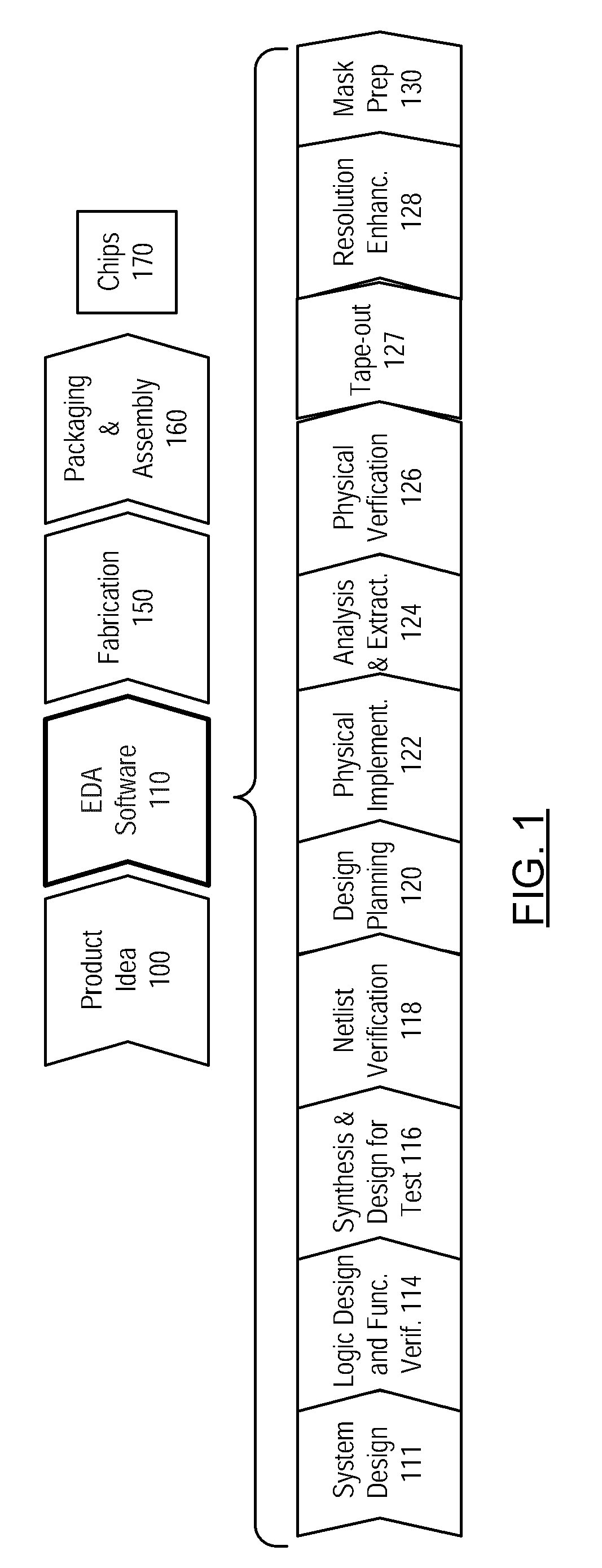
[0028]FIG. 1 is a simplified representation of an illustrative integrated circuit design flow. As with all flowcharts herein, it will be appreciated that many of the steps of FIG. 1 can be combined, performed in parallel or performed in a different sequence without affecting the functions achieved. In some cases a rearrangement of steps will achieve the same results only if certain other changes are made as well, and in other cases a rearrangement of steps will achieve the same results only if certain conditions are satisfied. Such rearrangement possibilities will be apparent to the reader.

[0029]At a high level, the process of FIG. 1 starts with the product idea (block 100) and is realized in an EDA (Electronic Design Automation) software design process (block 110). When the design is finalized, the fabrication process (block 150) and packaging and assembly proce...


PUM


Abstract

An EDA method is implemented for modifying a layout file after place and route. The method includes storing a library of shape modifications for cells in the design library used for implementation of the circuit. The library of shape modifications includes the results of process-specific calibration of the shape modifications which indicate adjustment of a circuit parameter caused by applying the shape modifications to the cells. The layout file is analyzed to identify a cell for adjustment of the circuit parameter. A shape modification calibrated to achieve the desired adjustment is selected from the library. The shape modification is applied to the identified cell in the layout file to produce a modified layout file. The modified layout file can be used for tape out, and subsequently for manufacturing of an improved integrated circuit.

Description

BACKGROUND OF THE INVENTION[0001]1. Field of the Invention[0002]The present invention relates to electronic design automation (EDA), and to implementation of layout changes for elements of integrated circuit designs for performance optimization.[0003]2. Description of Related Art[0004]Integrated circuit design is supported by electronic design automation. One approach to EDA supported design is based on the definition of an integrated circuit using a computer system as a netlist of circuit elements. Also, a cell library is provided that includes a number of cells that can be chosen for use in a physical implementation of the circuit elements in the netlist. The cell library has a finite number of choices for the circuit elements, as each cell in the library is pre-qualified for manufacturability and other factors. To implement the netlist, cells are selected from the library, placed in a layout space, and interconnections are defined among the cells. The selection of cells, placemen...

Claims


Application Information

Patent Timeline
Patent Type & Authority Patents(United States)
IPC IPC(8): G06F17/50
CPCG03F1/144G03F1/36G06F17/5081G06F30/398
Inventor CHEN, QIANGTIRUMALA, SRIDHAR
Owner SYNOPSYS INC
Why Eureka
Try Eureka