Differential signal pair transmission structure, wiring board and electronic module

a transmission structure and signal technology, applied in the field ofdifferential signal pair transmission structure, can solve the problems of parasitic inductance and parasitic capacitance, easy interference of internal signals of chips by noise, and increase in transmission distortion caused by noise, so as to reduce time skew during signal transmission within the circuit stack of the wiring board

Active Publication Date: 2013-10-08
VIA LABS INC
View PDF6 Cites 9 Cited by
  • Summary
  • Abstract
  • Description
  • Claims
  • Application Information

AI Technical Summary

Benefits of technology

[0008]The present invention is directed to a differential signal pair transmission structure adapted to a wiring board and transmit a differential signal pair. The impedance mismatch and the time skew during the signal transmission within the circuit stack of the wiring board can be reduced.
[0009]The present invention is directed to a wiring board, using a differential signal pair transmission structure to transmit a differential signal pair. The impedance mismatch and the time skew during the signal transmission within the circuit stack of the wiring board can be reduced.
[0010]The present invention is directed to an electronic module using a wiring board having a differential signal pair transmission structure to transmit a differential signal pair. The impedance mismatch and the time skew during the signal transmission within the circuit stack of the wiring board can be reduced.

Problems solved by technology

However, when the frequency of an electronic signal is increased to a high-frequency status, for example, beyond a gigahertz (GHz, i.e. one thousand million hertz), the internal signals of a chip would be easily interfered by noise, so that transmission distortion caused by the noise gets more significantly.
In fact, crosstalk phenomenon mainly comes from a coupling between two adjacent conductors and thereby results parasitic inductance and parasitic capacitance, and the crosstalk gets more seriously with increasing wiring layout density in the IC elements.
Thus, problems of time skew would occur in differential signal pair transmission.

Method used


Image

  • Differential signal pair transmission structure, wiring board and electronic module
  • Differential signal pair transmission structure, wiring board and electronic module
  • Differential signal pair transmission structure, wiring board and electronic module

Examples


Embodiment Construction

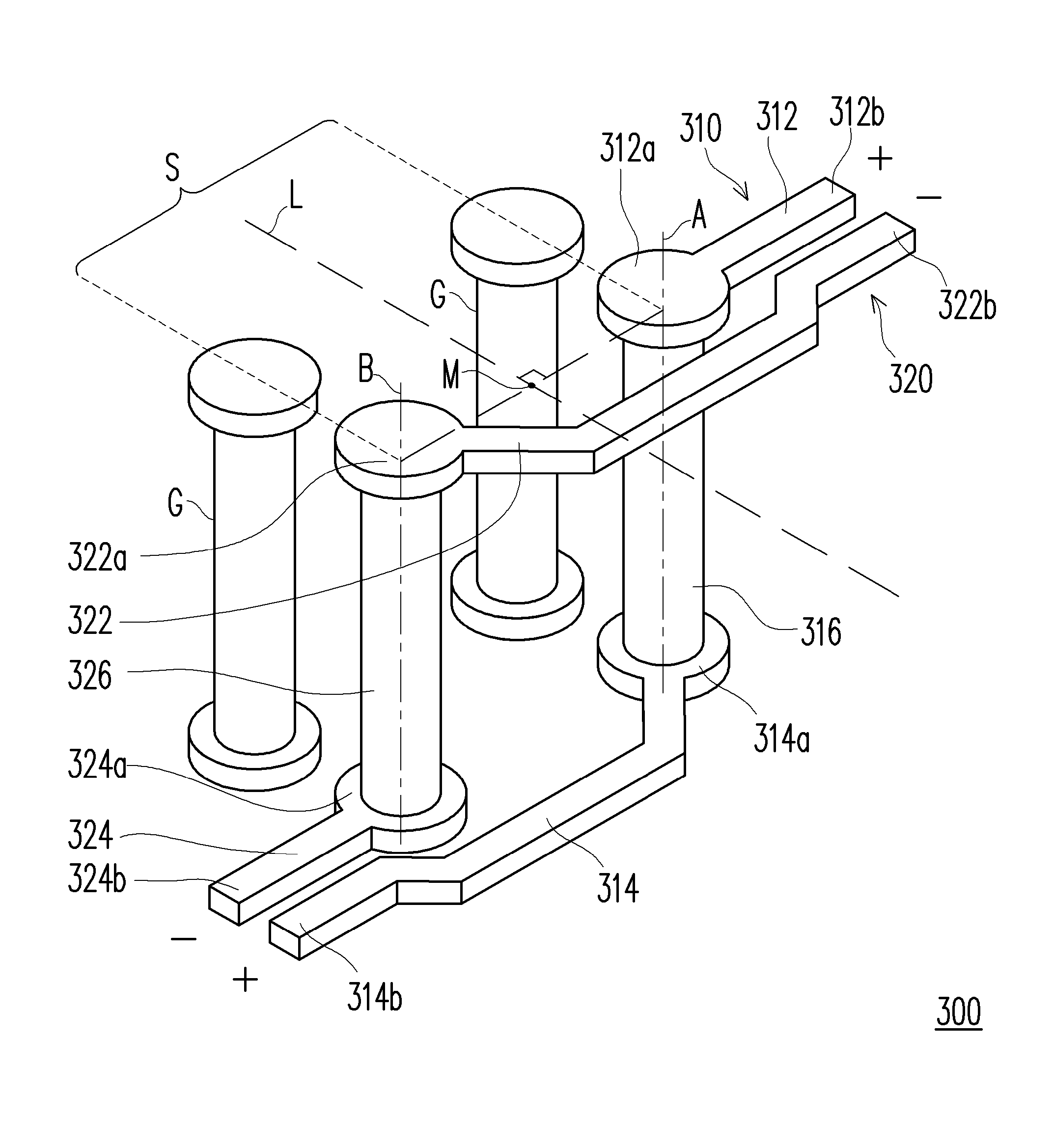
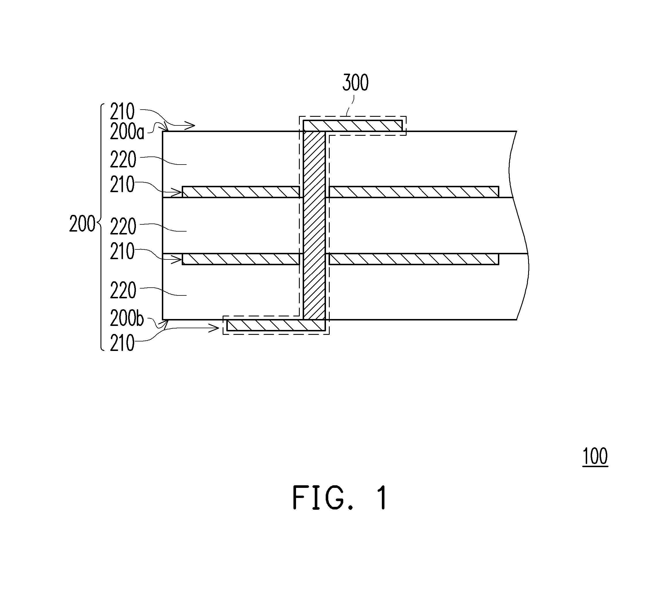
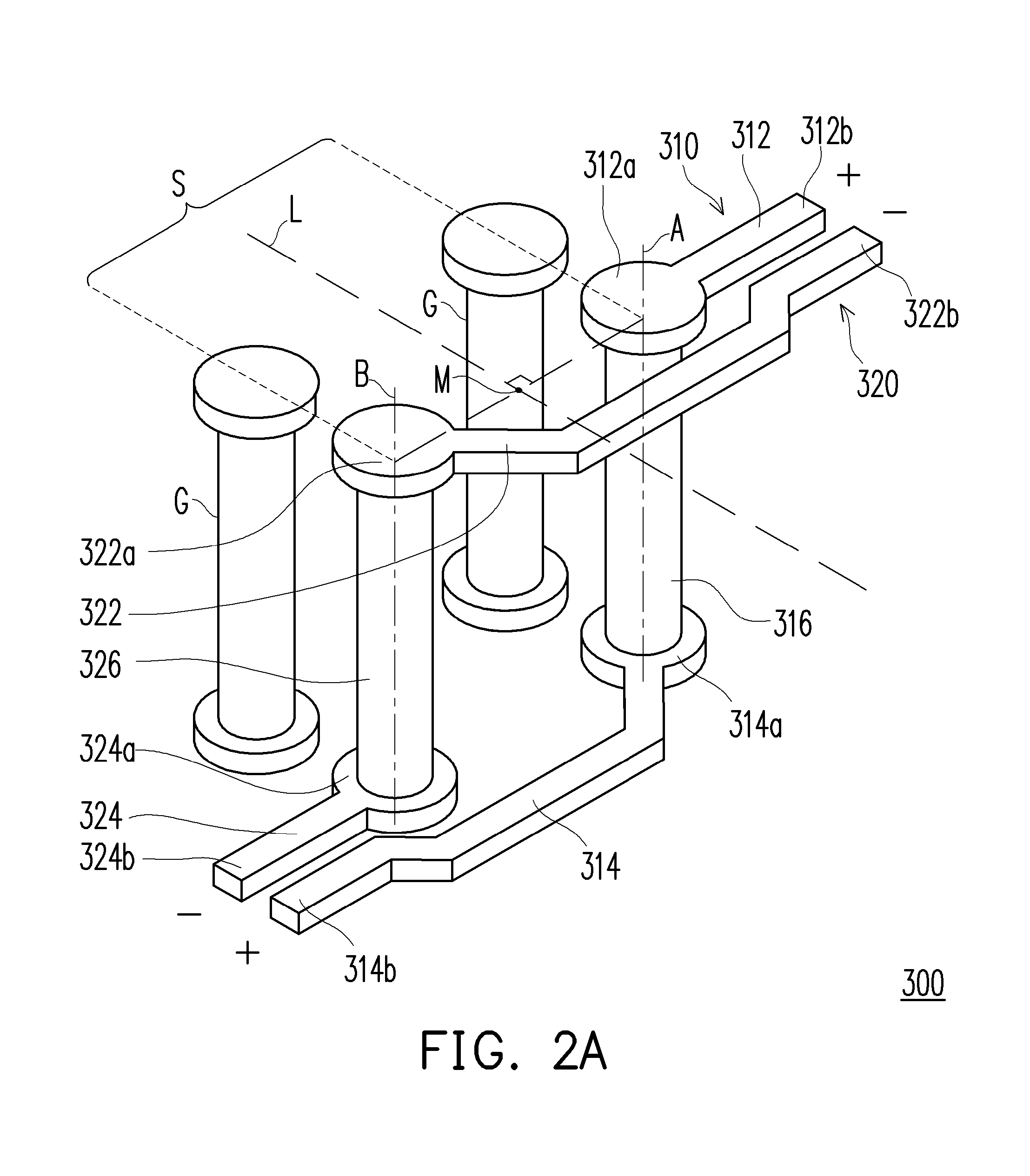
[0024]FIG. 1 is a cross-sectional view of a wiring board according to an embodiment of the present invention. Referring to FIG. 1, the wiring board 100 includes a circuit stack 200 and a differential signal pair transmission structure 300. The circuit stack 200 has an upper surface 200a and a lower surface 200b opposing to the upper surface 200a. The circuit stack 200 includes a plurality of patterned conductive layers 210 and a plurality of dielectric layers 220. The dielectric layers 220 are alternately disposed with the patterned conductive layers 210. Terminologies such as “upper” of the upper surface 200a and “lower” of the lower surface 200b are applicable to the embodiments shown and described in conjunction with the drawings. These terminologies are merely for the purposes of description and do not necessarily applied to the position or manner in which the invention may be constructed for actual use.

[0025]In the embodiment, a structure of three layers of the dielectric layer...


PUM


Abstract

A differential signal pair transmission structure adapted to a wiring board and including a first signal path and a second signal path is provided. The first signal path includes a first upper trace, a first lower trace and a first conductive through via. The second signal path includes a second upper trace, a second lower trace and a second conductive through via. A portion of the first signal path and a portion of the second signal path overlaps in the normal projection onto the upper or lower surface of the wiring board. Normal projections of the first and the second signal path projecting onto the upper surface of the wiring board are substantially symmetric with respect to a line which is perpendicular to a segment connecting normal projections of axes of the first and the second through via onto the upper surface and passes through the midpoint of the segment.

Description

CROSS-REFERENCE TO RELATED APPLICATION[0001]This application claims the priority benefits of U.S.A. provisional application Ser. No. 61 / 466,851, filed on Mar. 23, 2011 and Taiwan application serial No. 100124049, filed on Jul. 7, 2011. The entirety of each of the above-mentioned patent applications is hereby incorporated by reference herein and made a part of this specification.BACKGROUND OF THE INVENTION[0002]1. Field of the Application[0003]The present invention relates to a differential signal pair transmission structure, and more particularly, to a symmetric differential signal pair transmission structure and a wiring board and an electronic module utilizing the same.[0004]2. Description of Related Art[0005]In the semiconductor industry, it has become the tendency of the industry to develop integrated circuit (IC) elements with high integrity and high processing speed. Along with the steady advancements of integrated circuit element efficiency, the transmission frequency of elec...

Claims


Application Information

Patent Timeline
Patent Type & Authority Patents(United States)
IPC IPC(8): H05K1/16
CPCH05K1/0245H05K1/0251H05K1/0248H05K2201/09618H05K2201/09672
Inventor LEE, SHENG-YUAN
Owner VIA LABS INC
Why Eureka
Try Eureka