Method of forming an extremely thin semiconductor insulator (ETSOI) FET having a stair-shaped raised source/drain

a technology of semiconductor insulators and stair-shaped sources, applied in the field of field-effect transistors, can solve the problems of increasing leakage current and variability, increasing device dimensions, and bringing performance improvement, so as to reduce external resistance, increase parasitic resistance, and increase the extension resistance

Active Publication Date: 2013-11-05
GLOBALFOUNDRIES US INC
View PDF4 Cites 16 Cited by
  • Summary
  • Abstract
  • Description
  • Claims
  • Application Information

AI Technical Summary

Benefits of technology

[0009]In another aspect of the invention, a structure is provided that forms an MOSFET device having a stair-shape raised source / drain and extension. The thinner raised extension region next to a thin spacer on gate sidewall lowers the extension resistance without significantly increasing the parasitic resistance. Meanwhile, the thicker raised S / D further lowers the external resistance.
[0010]In another aspect of the invention, a single epitaxial growth is performed to form a thinner raised extension and thicker raised S / D simultaneously, thereby lowering the manufacturing cost as well as the contact resistance between the S / D and the extension thereof.

Problems solved by technology

Nevertheless, performance improvement brought up by this type of “classic” scaling, in device dimensions, has recently met obstacles and in some cases even been challenged, when the scaling goes beyond a certain point, by the increase in leakage current and variability that are inevitably associated with the continued reduction in device dimensions.
Shallow junctions are necessary to avoid lateral diffusion of implanted dopants into the channel, since such diffusion disadvantageously contributes to leakage currents and poor breakdown performance.
Due to the extremely thin SOI layer, the active SD and Extension regions experience create difficulties for dopant implants and activation annealing.
Although implants can be conducted, only partial dopants are activated due to lack of silicon re-crystallization.
The sheet resistance from both active regions is so elevated that its electrostatic performance is severely degraded.
Conventional raised S / D comes with the drawback of increased parasitic capacitance between the raised S / D and the gate.
However, the trade-off has to be made between two competing requirements—lowering external resistance and minimizing the increase of parasitic capacitance.

Method used


Image

  • Method of forming an extremely thin semiconductor insulator (ETSOI) FET having a stair-shaped raised source/drain
  • Method of forming an extremely thin semiconductor insulator (ETSOI) FET having a stair-shaped raised source/drain
  • Method of forming an extremely thin semiconductor insulator (ETSOI) FET having a stair-shaped raised source/drain

Examples


Embodiment Construction

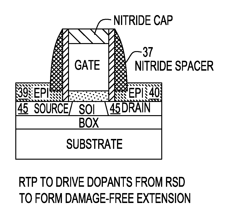
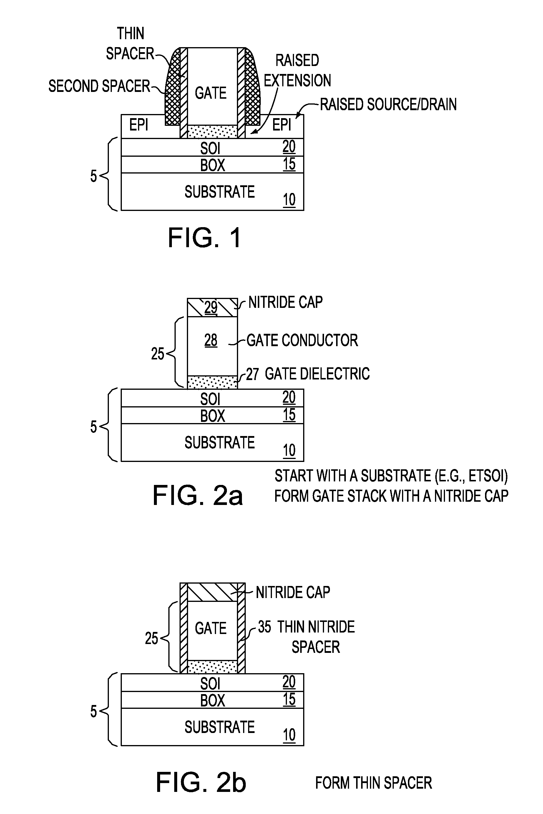
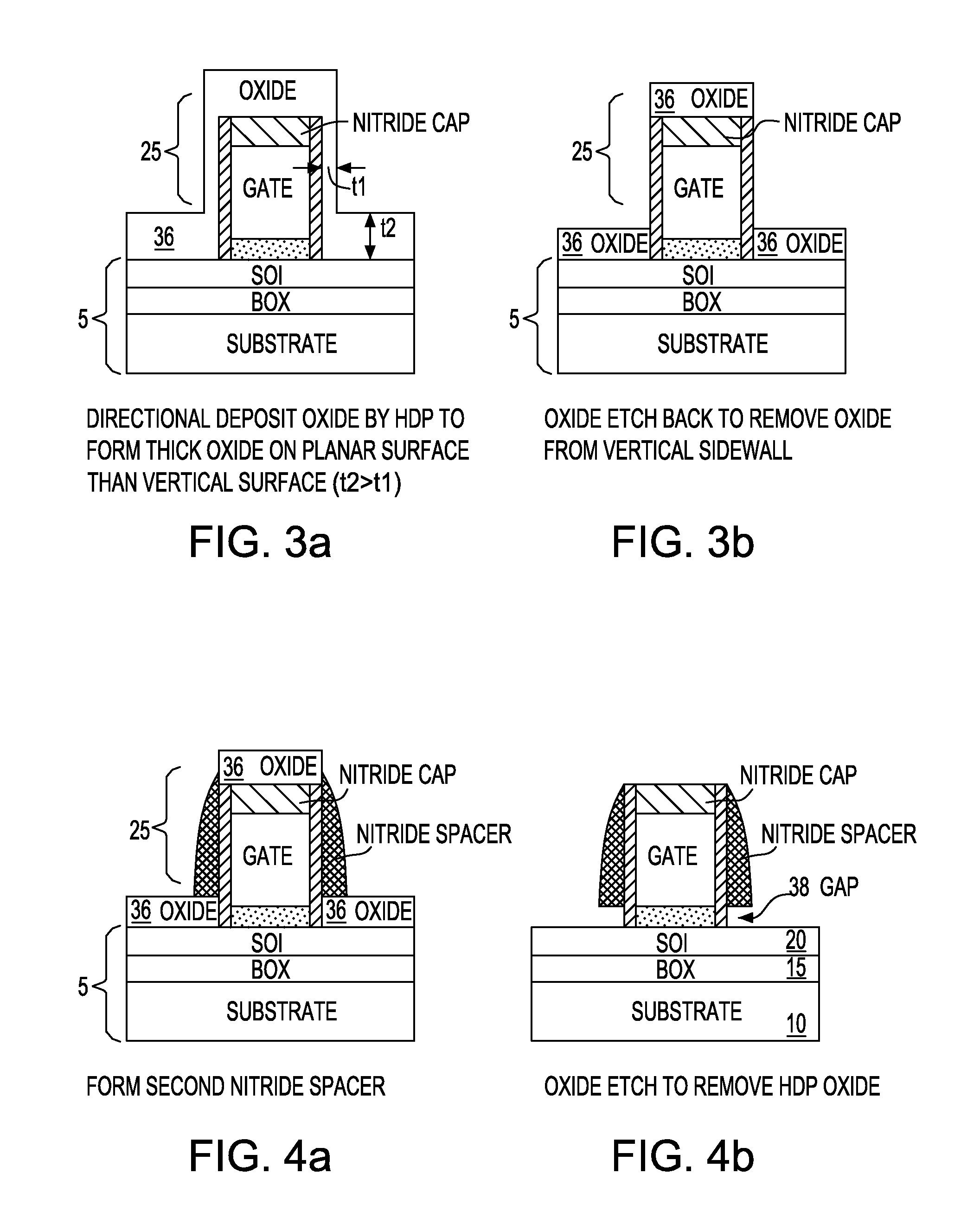
[0021]Detailed embodiments of the present invention are disclosed hereinafter. However, it is to be understood that they are merely illustrative of the invention that may be embodied in various forms. In addition, each of the examples given in connection with the various aspects of the invention is intended to be illustrative, and not restrictive. Further, the figures are not necessarily to scale, some features may be exaggerated to show details of particular components. Therefore, specific structural and functional details disclosed herein are not to be interpreted as limiting, but merely as a representative basis for teaching one skilled in the art to variously employ the present invention.

[0022]An illustrative structure and a method for forming semiconductor FET devices on a semiconductor-on-insulator (SOI) substrate are described having an extremely thin semiconductor-on-insulator layer. The extremely thin semiconductor-on-insulator (ETSOI) layer is present atop the buried insul...


PUM


Abstract

A MOSFET device is formed on top of a semiconductor-on-insulator (SOI) substrate having a semiconductor layer with a thickness ranging from 3 nm to 20 nm. A stair-shape raised extension, a raised source region and a raised drain region (S / D) are formed on top of the SOI substrate. The thinner raised extension region abuts at a thin gate sidewall spacer, lowering the extension resistance without significantly increasing the parasitic resistance. A single epitaxial growth forms the thinner raised extension and the thicker raised S / D preferably simultaneously, reducing the fabrication cost as well as the contact resistance between the raised S / D and the extension. A method of forming the aforementioned MOSFET device is also provided.

Description

FIELD OF THE INVENTION[0001]The present disclosure relates generally to semiconductor devices, and more specifically, to a field-effect transistor (FET) formed on a semiconductor-on-insulator (SOI) substrate having an epitaxial raised source and drain provided with an extension integrated thereon.BACKGROUND AND RELATED ART[0002]With shrinking dimensions of various integrated circuit components, transistors such as FETs have experienced dramatic improvements in both performance and power consumption. These improvements may be largely attributed to the reduction in dimensions of components used therein, which in general translate into reduced capacitance, resistance, and increased through-put current from the transistors. Nevertheless, performance improvement brought up by this type of “classic” scaling, in device dimensions, has recently met obstacles and in some cases even been challenged, when the scaling goes beyond a certain point, by the increase in leakage current and variabili...

Claims


Application Information

Patent Timeline
Patent Type & Authority Patents(United States)
IPC IPC(8): H01L21/84
CPCH01L29/66628H01L29/66772H01L29/78654
Inventor CHENG, KANGGUODORIS, BRUCE B.KHAKIFIROOZ, ALISHAHIDI, GHAVAM G.
Owner GLOBALFOUNDRIES US INC
Why Eureka
Try Eureka