MOS capacitors with a finfet process

a technology of finfet and capacitor, which is applied in the direction of capacitors, diodes, semiconductor devices, etc., can solve the problems of noise, change in voltage at the device, and substantial increase in the number of steps used in the fabrication process of decoupling capacitors

Active Publication Date: 2013-11-12
GLOBALFOUNDRIES US INC
View PDF13 Cites 26 Cited by
  • Summary
  • Abstract
  • Description
  • Claims
  • Application Information

AI Technical Summary

Benefits of technology

[0011]An integrated circuit is shown that includes at least one capacitor and at least one transistor. The at least one capacitor includes a first electrical terminal comprising a plurality of fins from doped semiconductor on a top layer of doped semiconductor on a semiconductor-on-insulator substrate; a second electrical terminal comprising an undoped material having a bottom surface shape that is complementary to the first electrical terminal such that an interface area between the first electrical terminal and the second electrical terminal is larger than a capacitor footprint; and a dielectric layer separating the first and second electrical terminals. The at least one transistor includes one or more fins, each having a semiconductor layer and an oxide layer; a gate comprising the undoped material, having a surface shape that is complementary to the one or more fins; and a dielectric layer separating the one of more fins and the gate.
[0012]An integrated circuit includes at least one capacitor formed on an insulator layer of a substrate and at least one transistor formed on the insulator layer of the substrate. The at least one capacitor includes a first electrical terminal comprising a plurality of fins formed from doped semiconductor on a layer of the doped semiconductor; a second electrical terminal comprising an undoped material having a bottom surface shape that is complementary to the first electrical terminal such that an interface area between the first electrical terminal and the second electrical terminal is larger than a capacitor footprint; and a high-k dielectric layer separating the first and second electrical terminals. The at least one transistor includes one or more fins, each having a semiconductor layer and an oxide layer; a gate comprising the undoped material, having a surface shape that is complementary to the one or more fins; and a high-k dielectric layer separating the one of more fins and the gate. A fin height of the at least one transistor is smaller than a combined height of the fins of the at least one capacitor and the layer of doped semiconductor.

Problems solved by technology

When the current demand for a device changes, the power supply does not respond instantly and, as a result, voltage at the device changes until the power supply can adapt.
When events take place that have a frequency higher than what can be accommodated by a voltage regulator, noise occurs.
However, previous circuit designs for decoupling capacitors substantially increase the number of steps used in the fabrication process and do not benefit from the steps used to create nearby fin field effect transistors.

Method used


Image

  • MOS capacitors with a finfet process
  • MOS capacitors with a finfet process
  • MOS capacitors with a finfet process

Examples


Embodiment Construction

[0031]The operation of decoupling capacitors is such that it is advantageous to place the capacitor as close as possible to a device that uses the decoupled signal. The longer the transmission line between the decoupling capacitor and the device, the larger the inductance, and a large inductance slows the response of the capacitor. It is therefore helpful to integrate the decoupling capacitors directly with an integrated circuit, such that the distance is minimized.

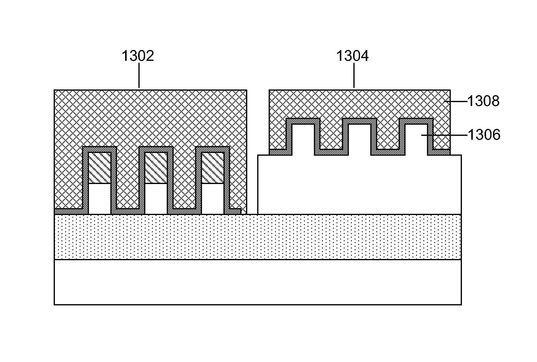
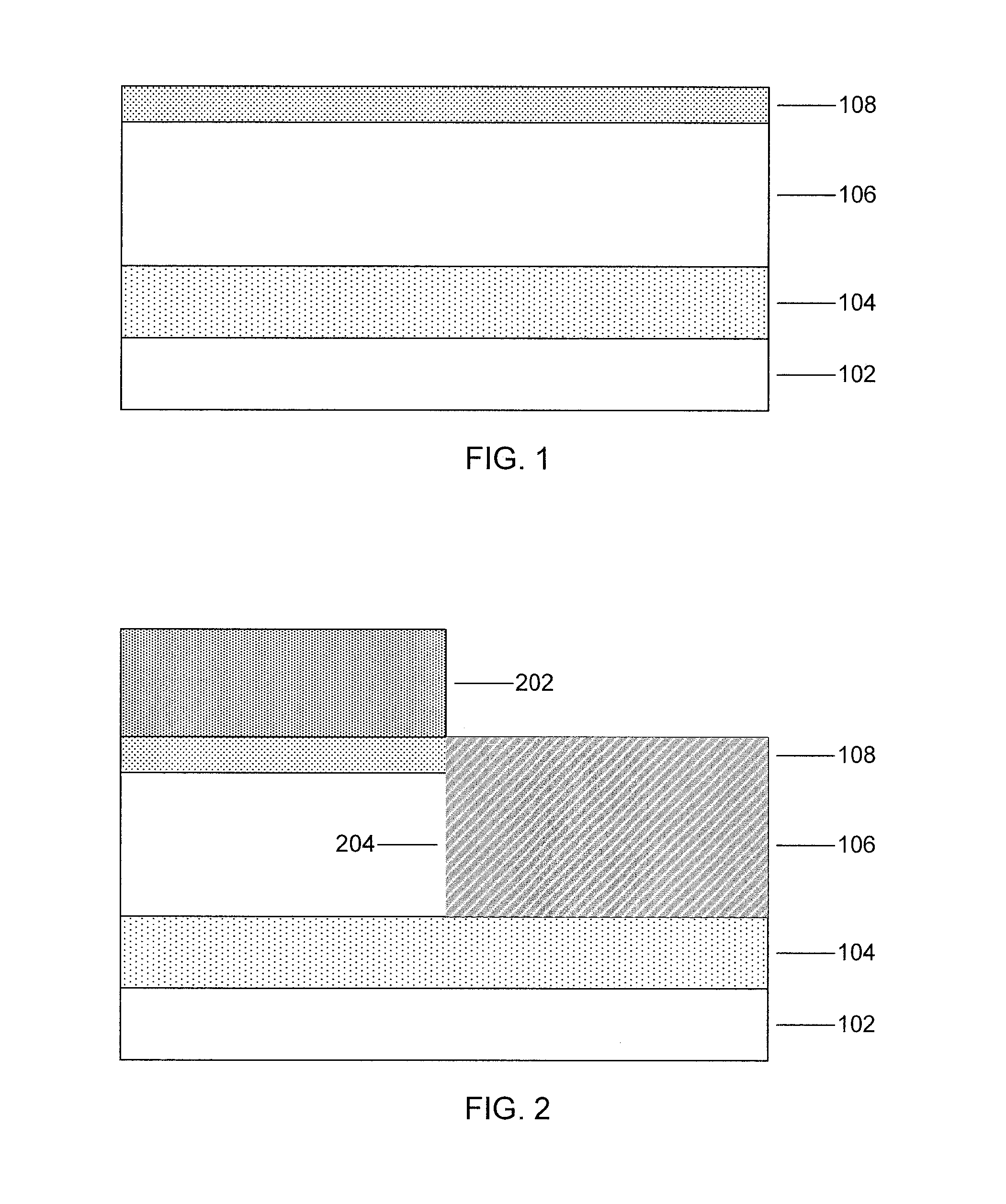
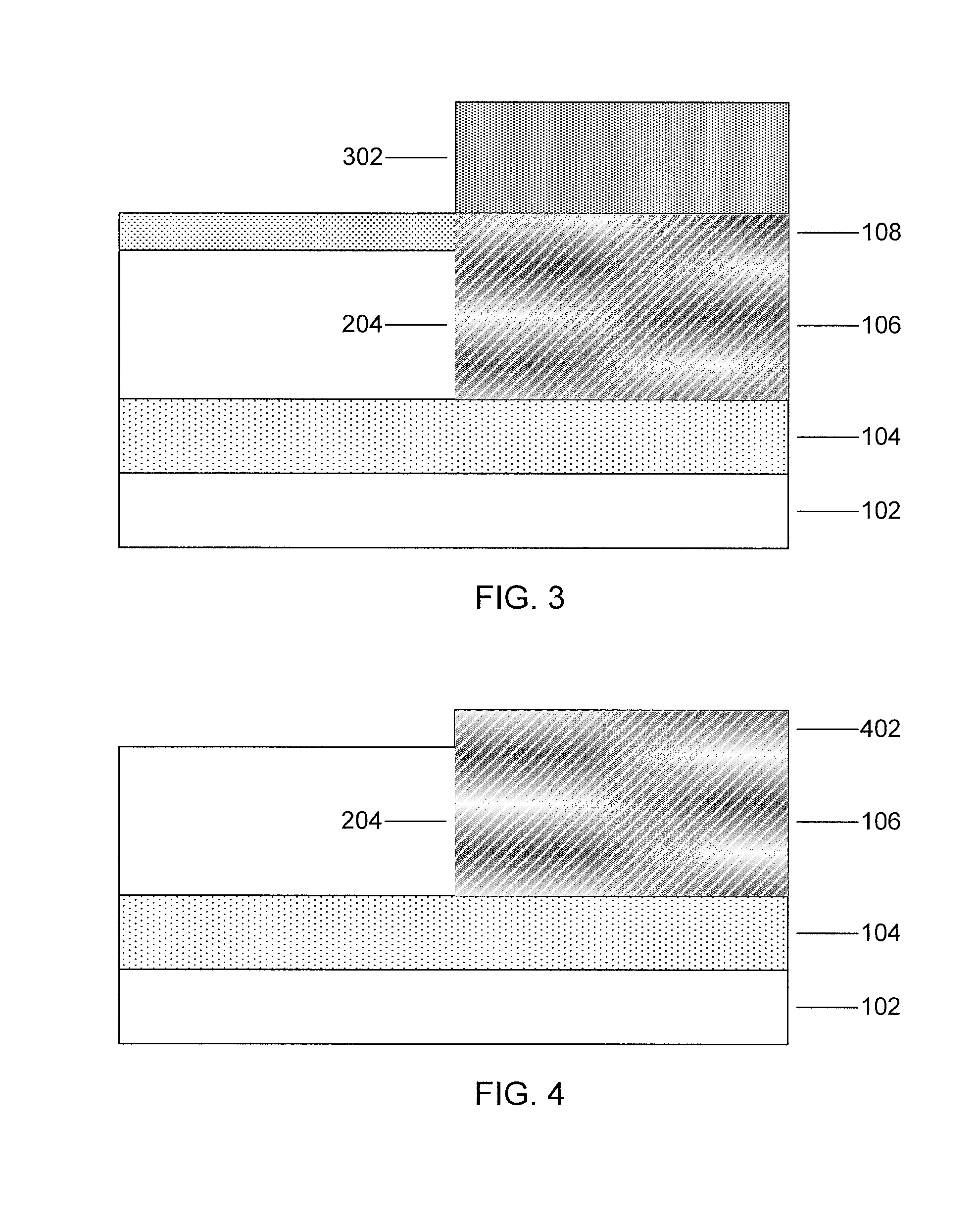
[0032]The present principles provide for the integration of decoupling capacitors in metal-oxide semiconductor (MOS) fin field effect transistor (FET) processes. In particular, the present principles form a doped region on a substrate to form one capacitor element and partially forms fins on the doped substrate to increase the capacitor area, without increasing the capacitor's footprint on the chip.

[0033]Increasing conductor area in a capacitor provides a corresponding increase in capacitance. This, along with the use of ...


PUM


Abstract

Capacitors include a first electrical terminal that has fins formed from doped semiconductor on a top layer of doped semiconductor on a semiconductor-on-insulator substrate; a second electrical terminal that has an undoped material having bottom surface shape that is complementary to the first electrical terminal, such that an interface area between the first electrical terminal and the second electrical terminal is larger than a capacitor footprint; and a dielectric layer separating the first and second electrical terminals.

Description

RELATED APPLICATION INFORMATION[0001]This application is a Continuation application of copending U.S. patent application Ser. No. 13 / 471,955 filed on May 15, 2012, incorporated herein by reference in its entirety.BACKGROUND[0002]1. Technical Field[0003]The present invention relates to capacitor fabrication and, more particularly, to forming finned capacitors as part of a fin field effect transistor fabrication process.[0004]2. Description of the Related Art[0005]Decoupling capacitors are used to shield circuit elements from noise generated by other circuit elements. Noise is directed through the capacitor, reducing the effect it has elsewhere. For example, changing power demands for a device may manifest as changing current demand. When the current demand for a device changes, the power supply does not respond instantly and, as a result, voltage at the device changes until the power supply can adapt. When events take place that have a frequency higher than what can be accommodated b...

Claims


Application Information

Patent Timeline
Patent Type & Authority Patents(United States)
IPC IPC(8): H01L27/108
CPCH01L21/84H01L27/1288H01L27/1211H01L21/823431H01L28/90H01L27/0629
Inventor CHENG, KANGGUOHARAN, BALASUBRAMANIAN S.PONOTH, SHOMSTANDAERT, THEODORUS E.YAMASHITA, TENKO
Owner GLOBALFOUNDRIES US INC
Why Eureka
Try Eureka