Organic EL display device and manufacturing method of the same

a technology of organic el and display device, which is applied in the direction of static indicating device, discharge tube luminescnet screen, instruments, etc., can solve the problems of thick regions adjacent to blue pixels, non-uniform or asymmetrical thickness, etc., and achieve uniformity or symmetry improvement, reduce imbalance in thickness of organic layer, and suppress non-uniform drying speed of applied solution

Active Publication Date: 2013-11-19
JOLED INC
View PDF10 Cites 18 Cited by
  • Summary
  • Abstract
  • Description
  • Claims
  • Application Information

AI Technical Summary

Benefits of technology

[0211]As described above, the common hole transport layer 16D made of a low molecular weight material is formed by a vapor deposition method over the entire surfaces of the hole transport layer 16BB and the red and green light-emitting layers 16CR and 16CG in the present embodiment, thus contributing to improved condition of the interface of the blue light-emitting layer 16CB in addition to the advantageous effects achieved by the first to third embodiments. This ensures improved efficiency in injecting holes into the blue light-emitting layer 16CB, thus allowing for the same layer 16CB to provide the values close to its original characteristics. That is, the present embodiment contributes to improved light emission efficiency and longer life of the blue organic EL element 10B, thus providing even higher light emission efficiency and longer life of the color organic EL display device having the red, green and blue organic EL elements 10R, 10G and 10B arranged and formed therein.
[0212]Further, a low molecular weight material is added to the red and green light-emitting layers 16CR and 16CG, thus making it easier to adjust the carrier balance between holes and electrons. This suppresses the reduction of electron injection characteristic and hole transport characteristic to the red and green light-emitting layers 16CR and 16CG resulting from the formation of the common hole transport layer 16D, blue light-emitting layer 16CB and electron transport layer 16E. That is, this keeps the reduction of light emission efficiency and life, increase in drive voltage and change in light emission chromaticity of the red and green organic EL elements 10R and 10G to a minimum.Fifth Embodiment
[0213]FIG. 18 illustrates the sectional configuration of the display region of an organic EL display device lB according to a fifth embodiment of the present disclosure. The organic EL display device lB is identical in configuration to the counterpart according to the fourth embodiment except that the common hole transport layer 16D is provided directly on the hole injection layer 16AB without providing the hole transport layer 16BB of the blue organic EL element 10B.
[0214]The organic layer 16 of the red organic EL element 10R includes, for example, the hole injection layer 16AR, hole transport layer 16BR, red light-emitting layer 16CR, common hole transport layer (second hole injection / transport layer) 16D, blue light-emitting layer 16CB, electron transport layer 16E and electron injection layer 16F that are stacked in this order from the side of the lower electrodes 14, as with the red organic EL element 10R according to the fourth embodiment. The organic layer 16 of the green organic EL element 10G includes, for example, the hole injection layer 16AG, hole transport layer 16BG, green light-emitting layer 16CG, common hole transport layer 16D, blue light-emitting layer 16CB, electron transport layer 16E and electron injection layer 16F that are stacked in this order from the side of the lower electrodes 14, as with the green organic EL element 10G according to the fourth embodiment. The organic layer 16 of the blue organic EL element 10B includes, for example, the hole injection layer 16AB, common hole transport layer 16D, blue light-emitting layer 16CB, electron transport layer 16E and electron injection layer 16F that are stacked in this order from the side of the lower electrodes 14 and differs from the counterpart according to the fourth embodiment in that there is no blue hole transport layer. Of these, the common hole transport layer 16D, blue light-emitting layer 16CB, electron transport layer 16E and electron injection layer 16F are provided as common layers to be shared among the red, green and blue organic EL elements 10R, 10G and 10B.
[0215]The organic EL display device according to the present embodiment provides even longer life of the blue organic EL element 10B in addition to the advantageous effect achieved by the fourth embodiment. Further, providing the common hole transport layer 16D directly on the hole injection layer 16AB of the blue organic EL element 10B contributes not only to reduced number of manufacturing process steps but also reduced cost.Module and Application Examples
[0216]A description will be given below of application examples of the organic EL display device described in the above embodiments. The organic EL display device according to any one of the above embodiments is applicable as a display device of electronic equipment across all disciplines adapted to display a video signal fed thereto from external equipment or generated therein including a television set, digital camera, laptop personal computer, PDA such as mobile phone and video camcorder.(Module)

Problems solved by technology

This leads to a non-uniform or asymmetrical thickness of the organic layer after drying, thus resulting in thick regions adjacent to the blue pixels.

Method used


Image

  • Organic EL display device and manufacturing method of the same
  • Organic EL display device and manufacturing method of the same
  • Organic EL display device and manufacturing method of the same

Examples


fifth embodiments

Second to Fifth Embodiments

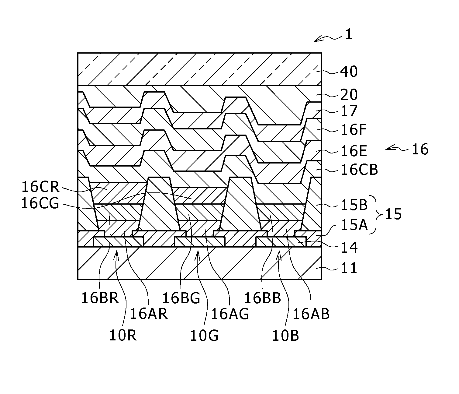
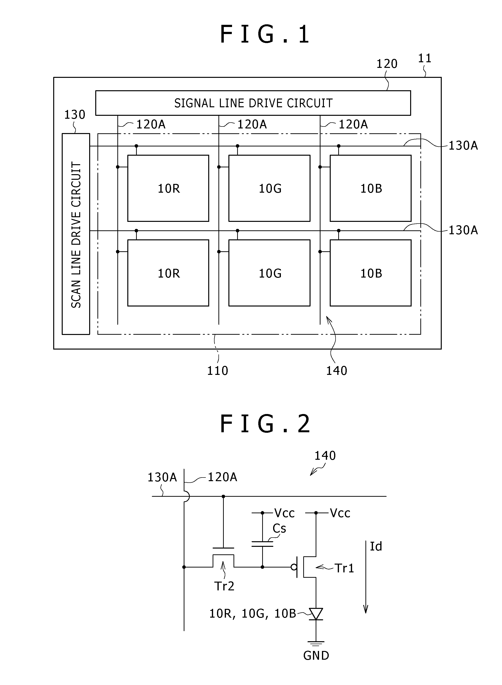
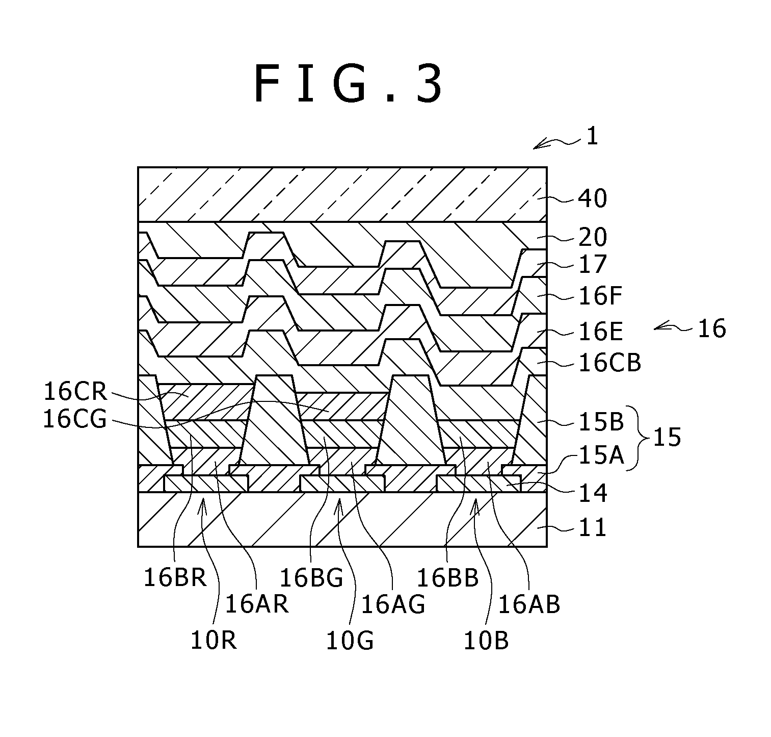
[0137]A description will be given below of second to fifth embodiments. Each of these embodiments relates to an element structure that particularly enhances the advantageous effect of the pixel arrangement described in the first embodiment with reference to FIGS. 4 to 9. On the other hand, the same components as those in the first embodiment are denoted by the same reference numerals, and the description thereof is omitted.

second embodiment

[0138]The second embodiment is identical in configuration to the first embodiment except that a low molecular weight material is included in the hole transport layer 16BB of the blue organic EL element 10B to provide improved blue light emission efficiency and longer life. Here, the term “low molecular weight material” means a substance other than those made of molecules of a high molecular weight polymer or condensate generated as a result of the repetition of the same or similar reactions of a low molecular weight compound in a chain-like manner, and refers to a compound practically having a single molecular weight. Further, heating does not practically generate any new chemical bond between molecules. Therefore, a low molecular weight material exists in the form of a single molecule.

[0139]Among specific materials that can be used as the hole transport layer 16BB are benzine, styrylamine, triphenylamine, porphyrin, triphenylene, azatriphenylene, tetracyanoquinodimethane, triazole,...

third embodiment

[0165]The third embodiment is identical in configuration to the second embodiment except that a low molecular weight material is included in the red and green light-emitting layers 16CR and 16CG.

[0166]The red and green light-emitting layers 16CR and 16CG are made of a mixture of two materials, a high molecular weight (light-emitting) material and a low molecular weight material added thereto. As a result, the present embodiment provides improved hole and electron injection efficiencies from the blue light-emitting layer 16CB serving as a common layer to the red or green light-emitting layer 16CR or 16CG. Here, the term “low molecular weight material” refers to a monomer or oligomer obtained by bonding two to 10 of this monomer together. A low molecular weight material having a weight-average molecular weight of 50000 or less is preferred. It should be noted that low molecular weight materials having a weight-average molecular weight beyond the above level are not necessarily exclude...


PUM


Abstract

Disclosed herein is an organic EL display device including, on a substrate: lower electrodes; first hole injection / transport layers; second organic light-emitting layers of colors other than blue; a blue first organic light-emitting layer; electron injection / transport layers; and an upper electrode.

Description

BACKGROUND[0001]The present disclosure relates to an organic EL (Electro Luminescence) display device that relies on the phenomenon of organic electroluminescence to emit light and a manufacturing method of the same.[0002]The advancement of the information and telecommunication industry at an accelerating pace has led to demand for display elements offering sophisticated performance. Among these, the organic EL element that is attracting attention as a next generation display device features not only a wide view angle and excellent contrast but also quick response time.[0003]The light-emitting layer and other layers forming an organic EL element are broadly classified into two types, namely, low and high molecular weight materials. It is commonly known that low molecular weight materials offer higher light emission efficiency and longer life. In particular, low molecular weight materials offer higher blue light performance.[0004]In order to form an organic film, on the other hand, a...

Claims


Application Information

Patent Timeline
Patent Type & Authority Patents(United States)
IPC IPC(8): H01L33/10
CPCH01L27/3218H01L51/0005H01L51/001H01L27/3213H01L27/3216H10K59/351H10K59/352H10K59/353H10K71/164H10K71/135
Inventor ANDO, MAKOTO
Owner JOLED INC
Why Eureka
Try Eureka