Method for manufacturing silicon oxide film, method for manufacturing semiconductor device, semiconductor device, display device and infrared light irradiating device

a manufacturing method and technology of silicon oxide film, applied in the direction of vacuum evaporation coating, chemical vapor deposition coating, coating, etc., can solve the problems of low quality and reliability of p-si tft, low film quality, and many problems of conventional semiconductor devices such as p-si

Inactive Publication Date: 2002-08-29
SEIKO EPSON CORP +1
View PDF0 Cites 23 Cited by
  • Summary
  • Abstract
  • Description
  • Claims
  • Application Information

AI Technical Summary

Benefits of technology

[0048] As described above, the present invention can improve conventional silicon oxide films of low quality (silicon oxide films formed by vapor deposition method, ultra-thin oxide films obtained by low-temperature oxidation method) to films of good quality by adding the step of infrared light irradiation; and at the same time, the present invention can improve interface conditions between a semiconductor and an oxide film. Moreover, when a semiconductor film is sandwiched between a first oxide film and a second oxide film, both interfaces can be improved. Furthermore, when the semiconductor is a crystalline film, this crystal can also be improved. As a result, superior effects will be realized: the electric characteristic of a semiconductor device, represented by a thin-film transistor, will increase; and at the same time, the operational stability and reliability of the semiconductor device will be enhanced.

Problems solved by technology

However, these conventional silicon oxide films have a problem in that the film quality is extremely low since electric charge trapped in oxide films is large, and the like.
As a result, if a conventional silicon oxide film is used as a gate insulating film of p-Si TFT, there is a problem in that only a p-Si TFT of low quality and reliability can be provided.
In other words, conventional semiconductor devices such as p-Si TFT have many problems because the quality of silicon oxide films is low.
The same problems are found in a micro-semiconductor device such as VLSI with an ultra-thin silicon oxide film.
More specifically, the problems are that a surface level and an oxide film trapping level are extremely high and the current of an oxide film is large.
These problems are the main causes in limiting the properties of a super-integrated circuit and shortening its life.
Thus, if an absorption ratio at a silicon oxide film is too low, the temperature of the silicon oxide film will not effectively increase but rather infrared light will be absorbed mainly by a substrate, thereby damaging the substrate.
However, if the oxidation temperature is below about 1,070.degree. C., the stress relaxation time will become much longer, so that the stress generated by oxidation will not be relaxed and remains in both thin films with an interface there-between.
As described above, the vapor deposition method is carried out under the temperature 600.degree. C. or below, so that oxidation stress during the period of ultra-thin oxide film formation cannot be relaxed.
This condition, however, cannot be satisfied with one irradiation when T.sub.ox is around 1,230.degree. C. or below.
This is because as a semiconducting material melts, adverse phenomena will occur: the change in an impurity concentration in the semiconductor material, the increase in interface states due to the random reconstruction of the interface between the oxide and semiconductor films, or, as the worst case, the destruction of the semiconductor device due to the evaporation and drift of the semiconducting material.
As a result, dangling bonds have worse semiconductor characteristics.
If the irradiation time is long, oxygen in the air will diffuse to an interface, so that there is a fear that a new low-temperature oxide will be formed during the cooling step of a semiconducting material.
As a result, improved characteristics of the interface will deteriorate again.

Method used


Image

  • Method for manufacturing silicon oxide film, method for manufacturing semiconductor device, semiconductor device, display device and infrared light irradiating device
  • Method for manufacturing silicon oxide film, method for manufacturing semiconductor device, semiconductor device, display device and infrared light irradiating device
  • Method for manufacturing silicon oxide film, method for manufacturing semiconductor device, semiconductor device, display device and infrared light irradiating device

Examples


first embodiment

[0070] First Embodiment

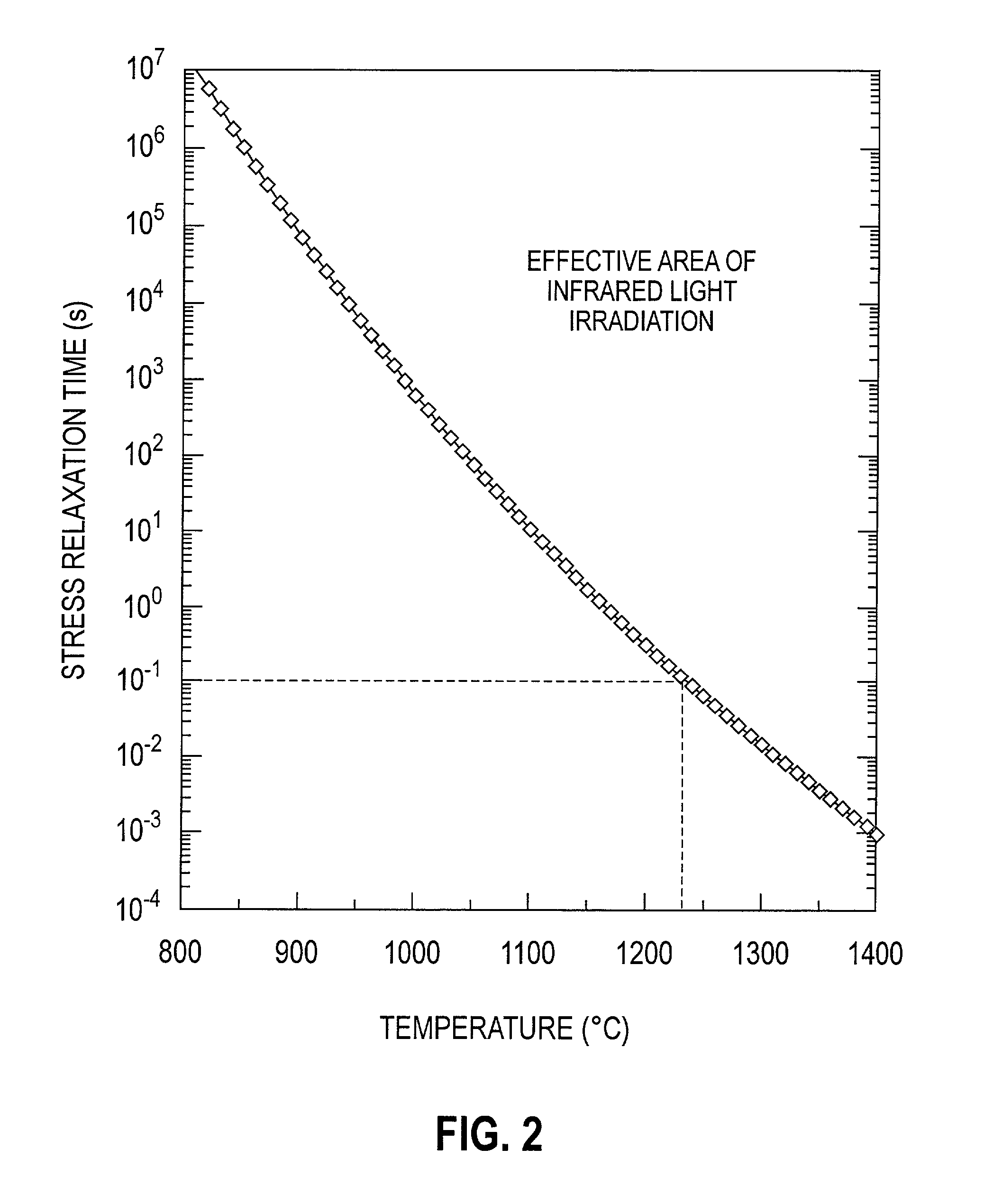
[0071] FIG. 4 is a figure showing the oxide film temperature changes by infrared light irradiation. As infrared light, a carbon dioxide laser beam was used and this infrared light was irradiated onto a silicon oxide film constituting a gate insulating film; temperature changes over the silicon oxide film were estimated by an electronic computer. The vertical line indicates the temperature of the silicon oxide film surface, and the horizontal line indicates the time right after irradiation has started. As a substrate, popular non-alkali glass is assumed. On a substrate, a silicon oxide film is deposited as an underlying layer-protecting film at the thickness of 200 nm by an ECR-PECVD method, and a polycrystalline silicon film with a thickness of 50 nm thereon and, moreover, a silicon oxide film as a gate insulating film with a thickness of 100 nm thereon are deposited by the ECR-PECVD method. The optical characteristics of the gate insulating film and the under...

second embodiment

[0075] Second Embodiment

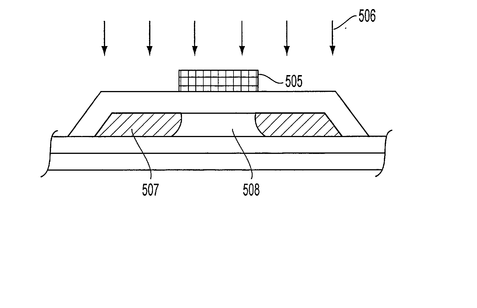
[0076] FIGS. 5(a)-(d) are figures showing, in cross section, the manufacturing process of a thin film semiconductor device for fabricating MOS field-effect transistors. In the Second Embodiment, a popular non-alkali glass having a strain point of about 650.degree. C. is used as a substrate 501.

[0077] First, a first silicon oxide film is deposited at about 200 nm by a ECR-PECVD method on the substrate 501, thus preparing an underlying layer-protecting film 502. The deposition conditions of the first silicon oxide film by the ECR-PECVD method are as follows:

[0078] Monosilane (SiH.sub.4) flow rate: 60 sccm;

[0079] Oxygen (O.sub.2) flow rate: 100 sccm;

[0080] Pressure: 2.40 m Torr;

[0081] Microwave (2.45 GHz) power: 2,250W;

[0082] Applied magnetic field: 875 Gauss;

[0083] Substrate temperature: 100.degree. C.; and

[0084] Film-forming time: 40 seconds.

[0085] On this underlying layer-protecting film, an intrinsic amorphous silicon film is deposited at the film thickness ...

third embodiment

[0115] Third Embodiment

[0116] Using the NMOS thin film semiconductor device obtained in the Second Embodiment as a switching element for picture elements of a color LCD having 200 (row).times.320(column).times.3(color)=192,000 (picture elements), an active matrix substrate was manufactured wherein a 6-bit digital data driver (column side driver) and a scanning driver (row side driver) were built-in the CMOS thin film semiconductor device obtained in the Second Embodiment.

[0117] FIG. 6 is a circuit diagram of the 6-bit digital data driver. The digital data driver of the Third Embodiment includes a clock signal line and a clock generating circuit, a shift resistor circuit, a NOR gate, a digital image signal line, a latch circuit 1, a latch pulse line, a latch circuit 2, a reset line 1, an AND gate, a reference potential line, a reset line 2, a 6-bit D / A converter by capacitance split, a CMOS analog switch, a common potential line and a source line reset-transistor. The output from the...


PUM

PropertyMeasurementUnit
thicknessaaaaaaaaaa
wavelengthaaaaaaaaaa

Abstract

The method for manufacturing a silicon oxide film is characterized in that the method includes the steps of forming the silicon oxide film by a vapor deposition method or the like and of irradiating infrared light onto this silicon oxide film. Thus, according to the present invention, a silicon oxide film of relatively low quality formed at relatively low temperature can be improved to be a silicon oxide film of high quality. When the present invention is applied to a thin-film semiconductor device, a semiconductor device of high operational reliability and high performance can be manufactured.

Description

[0001] The present invention relates to a method for manufacturing a silicon oxide film of good quality by a vapor deposition method. This silicon oxide film is suitable for an underlying layer-protecting film, a gate insulating film, an inter-layer insulating film, etc. The present invention also relates to a method for manufacturing a micro-semiconductor device of good quality (for example, metal / oxide film / semiconductor field effect transistor (MOSFET)) wherein a semiconductor surface is oxidized at a relatively low temperature of, e.g., about 800.degree. C. or less and an extra-thin silicon oxide film (having less than about 10 nm in film thickness) of good quality is then formed. The present invention also relates to a method for manufacturing a semiconductor device (for instance, a thin film transistor) of high performance and reliability at a relatively low temperature such as around 600.degree. C. or below. Moreover, the present invention relates to a semiconductor device of...

Claims


Application Information

Patent Timeline
Patent Type & Authority Applications(United States)
IPC IPC(8): C23C14/10C23C14/58C23C16/40C23C16/56H01L21/316H01L29/49
CPCC23C14/10C23C14/58C23C14/5813C23C16/402C23C16/56H01L21/02164H01L21/02211H01L21/02238H01L21/02252H01L21/02274H01L21/02304H01L21/02315H01L21/0234H01L21/02362H01L21/268H01L21/28158H01L21/3003H01L21/3105H01L29/4908
Inventor MIYASAKA, MITSUTOSHISAKAMOTO, TAKAO
Owner SEIKO EPSON CORP
Why Eureka
Try Eureka