Semiconductor device having SOI substrate

a technology of semiconductor devices and substrates, which is applied in the direction of semiconductor devices, basic electric elements, electrical appliances, etc., can solve the problems of complex manufacturing process and complicated manufacturing process of semiconductor devices, and achieve the effects of preventing breakdown voltage reduction, reducing device dimensions, and high breakdown voltag

Inactive Publication Date: 2013-12-10
DENSO CORP
View PDF6 Cites 5 Cited by
  • Summary
  • Abstract
  • Description
  • Claims
  • Application Information

AI Technical Summary

Benefits of technology

[0009]In view of the above-described problem, it is an object of the present disclosure to provide a semiconductor device having a SOI substrate and a method for manufacturing the same. A breakdown voltage of the device is improved.
[0011]In the above device, the second conductive type regions sandwich the first conductive type region so that the second conductive type regions are spaced apart from each other by a predetermined distance. The first and second conductive type regions are disposed in the part of the active layer adjacent to the embedded insulation film and under the semiconductor element. Accordingly, a charge is induced to a part of the second conductive type regions adjacent to the insulation film. Specifically, no charge is induced to a part of the first conductive type regions adjacent to the insulation film. Thus, a reverse layer is localized in the part of the second conductive type regions. Accordingly, a pseudo field plate is formed. Thus, a voltage drop is generated in accordance with a distance of the first conductive type region in a lower portion of the active layer adjacent to the insulation film. Without forming concavity and convexity having a large depth, the breakdown voltage is improved.
[0013]In the above device, the second conductive type regions sandwich the first conductive type region so that the second conductive type regions are spaced apart from each other by a predetermined distance. The first and second conductive type regions are disposed in the part of the active layer adjacent to the embedded insulation film and under the semiconductor element. Accordingly, a charge is induced to a part of the second conductive type regions adjacent to the insulation film. Specifically, no charge is induced to a part of the first conductive type regions adjacent to the insulation film. Thus, a reverse layer is localized in the part of the second conductive type regions. Accordingly, a pseudo field plate is formed. Thus, a voltage drop is generated in accordance with a distance of the first conductive type region in a lower portion of the active layer adjacent to the insulation film. Thus, the equivalent electric potential lines extends in the vertical direction toward the first conductive type region, and therefore, the distance between the equivalent electric potential lines is compensated. Thus, the breakdown voltage is improved. Without forming concavity and convexity having a large depth, the breakdown voltage of the device is improved.
[0015]In the above method, the second conductive type regions sandwich the first conductive type region so that the second conductive type regions are spaced apart from each other by a predetermined distance. The first and second conductive type regions are disposed in the part of the active layer adjacent to the embedded insulation film and under the semiconductor element. Accordingly, a charge is induced to a part of the second conductive type regions adjacent to the insulation film. Specifically, no charge is induced to a part of the first conductive type regions adjacent to the insulation film. Thus, a reverse layer is localized in the part of the second conductive type regions. Accordingly, a pseudo field plate is formed. Thus, a voltage drop is generated in accordance with a distance of the first conductive type region in a lower portion of the active layer adjacent to the insulation film. Thus, the equivalent electric potential lines extends in the vertical direction toward the first conductive type region, and therefore, the distance between the equivalent electric potential lines is compensated. Thus, the breakdown voltage is improved. Without forming concavity and convexity having a large depth, the breakdown voltage of the device is improved.
[0017]In the above device, the electric potential of the surface portion of the semiconductor element region is gradually reduced from the first impurity layer as a high potential side to the second impurity layer as a low potential side since the voltage drop is generated by the inner resistance of the electrode pattern. Further, the electric potential of each electric potential control region on the side of the semiconductor element region is reduced in a stepwise manner from the first impurity layer as a high potential side to the second impurity layer as a low potential side since the voltage drop is generated by the inner resistance of the electrode pattern. Accordingly, since the electric potential of the semiconductor element region from the first impurity layer to the second impurity layer is reduced, the electric potential of each electric potential control region disposed on the side of the semiconductor element region and the electric potential of the surface portion of the semiconductor element region are reduced. Accordingly, the electric field at both ends of the first and second impurity layers along with the longitudinal direction is restricted from concentrating. Thus, the breakdown voltage reduction is prevented. Further, the electric potential of each electric potential control region disposed on the side of the semiconductor element region can be controlled to be different from each other by using the electrode pattern. Accordingly, it is not necessary to form a control device such as a conventional dividing diode around the semiconductor element region. Accordingly, the dimensions of the device is reduced, and the electric field concentration at the periphery of the high breakdown voltage device is restricted. Thus, the device has a high breakdown voltage.

Problems solved by technology

Thus, a manufacturing process is complicated.
Thus, the manufacturing process of the device is complicated.

Method used


Image

  • Semiconductor device having SOI substrate
  • Semiconductor device having SOI substrate
  • Semiconductor device having SOI substrate

Examples


first embodiment

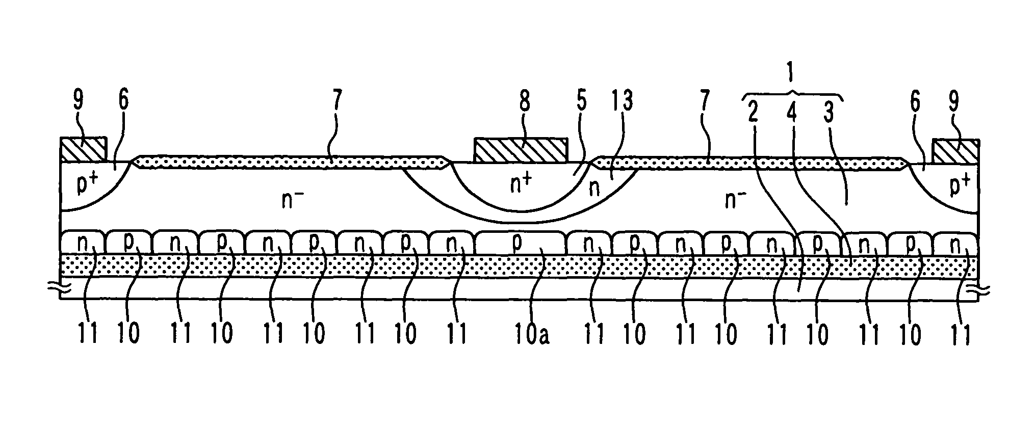
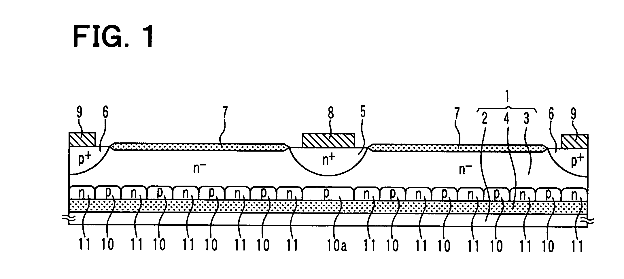
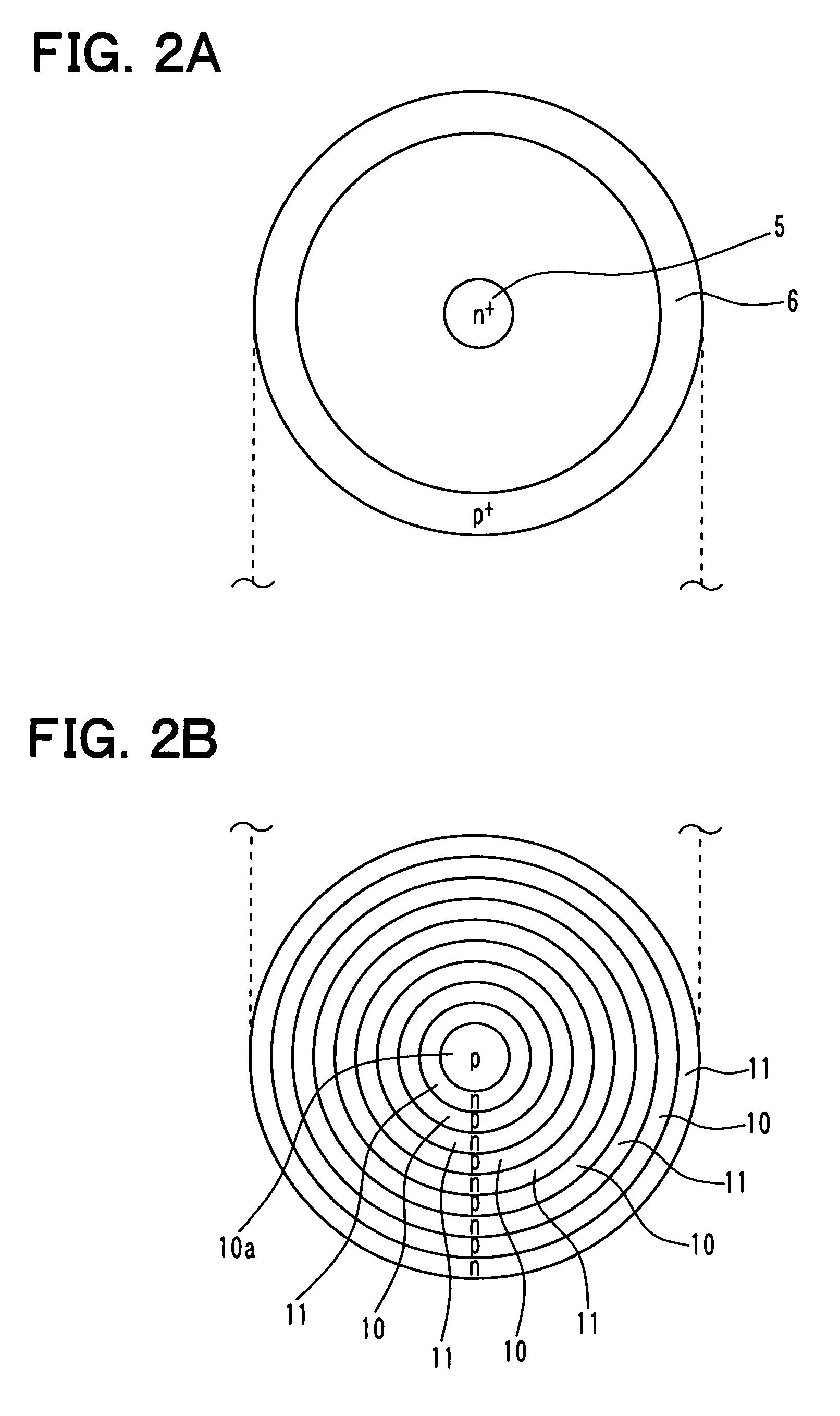
[0060]First embodiment will be explained. In the first embodiment, a semiconductor device has a lateral PN diode as a semiconductor element. FIG. 1 shows a cross sectional view of the semiconductor device. FIGS. 2A and 2B are a top surface layout and a backside surface layout of the device.

[0061]As shown in FIG. 1, the device is formed from a SOI substrate 1. The substrate 1 is prepared such that a support substrate 2 made of a silicon substrate and an active layer 3 are bonded to each other via an embedded insulation film 4. The embedded insulation film 4 is made of an oxide film or the like. The active layer 3 is prepared such that a N− type silicon substrate is thinned. The active layer 3 is divided into multiple element separation regions by an element separation structure. The PN diode is formed in one element separation region surrounded with the element separation structure.

[0062]The thickness of the active layer 3 is, for example, 5 to 25 micrometers. A N+ type cathode regio...

second embodiment

[0086]A second embodiment will be explained.

[0087]FIG. 6 shows a semiconductor device according to the present embodiment. FIGS. 7A and 7B show an layout view and a lower layout view of the device. In the device, a trench separation structure 20 for surrounding the outer periphery of the anode region 6 is formed. The trench separation structure 20 includes a groove 21 and an insulation film 22. The groove 21 is formed on the surface of the active layer 3, and reaches the embedded insulation film 4. The insulation film 22 is filled in the groove 21. For example, a mask formed by the photo etching method is used for etching the active layer 3 so that the groove 21 is formed. Then, the insulation film 22 is filled in the groove 21 such that a thermal oxidation process is performed, or an insulation material is deposited in the groove 21. Thus, the insulation material is filled in the groove 21. Thus, the trench separation structure 20 is formed.

[0088]The trench separation structure 20 ...

third embodiment

[0089]A third embodiment will be explained.

[0090]FIG. 8 shows a semiconductor device according to the present embodiment. FIGS. 9A and 9b show an upper layout view and a lower layout view of the semiconductor device. In the semiconductor device, a resistance type field plate 30 is formed on the PN diode via a LOCOS oxide film 7. The resistance type field plate 30 is made of, for example, a high resistance layer such as non-doped poly silicon. The resistance type field plate 30 extends in a spiral manner around the cathode region 5 as a center, and reaches the anode region 6.

[0091]In the resistance type field plate 30, a voltage drop according to the distance of the high resistance layer is generated between the cathode region 5 having the high electric potential and the anode region 6. The voltage drop is caused by an inner resistance of the high resistance layer. Accordingly, the voltage drops proportionally along with the radial direction around the cathode region 5 as the center ...


PUM


Abstract

A semiconductor device includes: a SOI substrate; a semiconductor element having first and second impurity layers disposed in an active layer of the SOI substrate, the second impurity layer surrounding the first impurity layer; and multiple first and second conductive type regions disposed in a part of the active layer adjacent to an embedded insulation film of the SOI substrate. The first and second conductive type regions are alternately arranged. The first and second conductive type regions have a layout, which corresponds to the semiconductor element.

Description

CROSS REFERENCE TO RELATED APPLICATIONS[0001]This application is based on Japanese Patent Applications No. 2009-227157 filed on Sep. 30, 2009, No. 2009-232421 filed on Oct. 6, 2009, and No. 2010-177427 filed on Aug. 6, 2010, the disclosures of which are incorporated herein by reference.FIELD OF THE INVENTION[0002]The present invention relates to a semiconductor device having a SOI substrate and a method for manufacturing the same. The semiconductor device has a sufficient breakdown voltage.BACKGROUND OF THE INVENTION[0003]Conventionally, a semiconductor device has a semiconductor element, which is formed in a SOI substrate. The SOI substrate is prepared such that a support substrate and an active layer are bonded to each other via an embedded insulation film. In the semiconductor device, a potential of the support substrate is fixed to be a predetermined potential such as a GND potential when the device is operated. Under a condition that the potential of the support substrate is fi...

Claims


Application Information

Patent Timeline
Patent Type & Authority Patents(United States)
IPC IPC(8): H01L29/66
CPCH01L21/76264H01L21/84H01L27/1203H01L29/0634H01L29/404H01L29/405H01L29/407H01L29/408H01L29/66128H01L29/7394H01L29/7824H01L29/8611H01L29/0657H01L29/0692H01L29/1608
Inventor ASHIDA, YOUICHITOKURA, NORIHITOTAKAHASHI, SHIGEKINAKAYAMA, YOSHIAKISHIRAKI, SATOSHISENDA, KOUJI
Owner DENSO CORP
Why Eureka
Try Eureka