Conductive interconnects

a technology of interconnects and conductive materials, applied in the field of conductive interconnects, can solve problems such as cost and practical difficulties, and achieve the effect of increasing the manufacturing yield of the process

Inactive Publication Date: 2013-12-10
HEWLETT PACKARD DEV CO LP
View PDF11 Cites 3 Cited by
  • Summary
  • Abstract
  • Description
  • Claims
  • Application Information

AI Technical Summary

Benefits of technology

[0008]By electrodepositing the dielectric material on the first interconnect, the dielectric is self-aligned to the underlying conductor, with the shape and position of both the metal conductor and the overlying electrodeposited dielectric material determined by the trench defined by the original multilevel dielectric structure. This avoids problems with previous techniques such as photo- or laser patterning of a polymer material, which require a certain level of pattern re-alignment that may cause practical difficulties and cost when applied to large area polymer substrates because of dimensional instability.
[0009]The technique of electrodepositing the gate or crossover dielectric may produce a continuous film without pinhole or other defects which would effect a short between the gate and source / drain (in a TFT) or between conductor A and conductor B in a crossover, potentially increasing the manufacturing yield of the process.

Problems solved by technology

This avoids problems with previous techniques such as photo- or laser patterning of a polymer material, which require a certain level of pattern re-alignment that may cause practical difficulties and cost when applied to large area polymer substrates because of dimensional instability.

Method used


Image

  • Conductive interconnects
  • Conductive interconnects
  • Conductive interconnects

Examples


Embodiment Construction

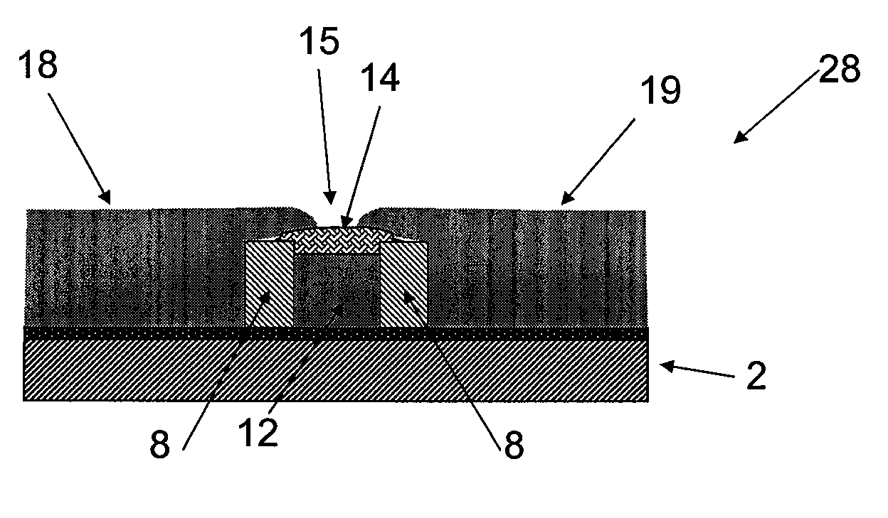
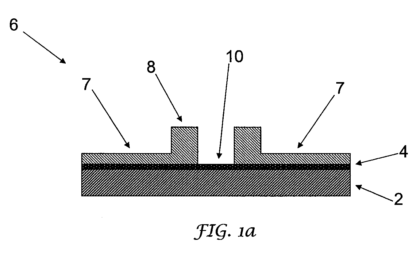
[0017]Referring to FIG. 1a a carrier 2, for example a film of a plastics material, has a conductive surface 4. A multilevel dielectric structure 6 is formed on the conductive surface 4, for example by photolithography using a material such as SU8, or by UV micromoulding. The dielectric structure 6 includes a pair of upstanding walls 8 which define a trench 10 between them, and regions of dielectric material 7 outside the trench 10 and adjacent to the walls 8. The base of the trench 10 comprises part of the conductive surface 4 between the walls 8. If UV micromoulding is used to form the dielectric structure 6, then the base of the trench 10 may be cleared of any residue by plasma, or UV ozone ashing to ensure that it is presents a conductive surface.

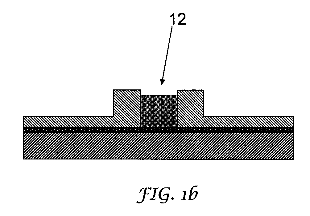
[0018]In FIG. 1b, the carrier is placed in a standard electroforming system, where the conductive layer 4 forms the cathode. A metal (typically nickel, gold, copper or a combination thereof is deposited to form a first conductive interco...


PUM

PropertyMeasurementUnit
conductiveaaaaaaaaaa
semiconductoraaaaaaaaaa
dielectricaaaaaaaaaa

Abstract

A method of making a conductive interconnect structure includes the steps of: electrodepositing a metal on a conductive surface (4) of a carrier (2) to form a first elongate conductive interconnect (12); and electrodepositing a dielectric material (14) on said conductive interconnect (12) while the conductive interconnect (12) is in contact with the conductive surface (4).

Description

RELATED APPLICATIONS[0001]The present application is based on, and claims priority from, United Kingdom Application Number 0722613.7, filed Nov. 19, 2007, the disclosure of which is hereby incorporated by reference herein in its entirety.FIELD OF THE INVENTION[0002]The present invention relates to conductive interconnects.BACKGROUND TO THE INVENTION[0003]Displays which are based on electro-optical effects such as LCDs, OLEDs, and electrophoretic displays are often addressed using an array of ‘active’ devices. These provide a non-linear disconnection between the matrixing of the information and the electric field or current at each pixel. Typically a thin film transistor (TFT) is used such that its gate is controlled in parallel with all other devices on a particular row, and its source is provided by a data driver connected to each column. The drain is connected to the pixel driving electrode and optionally a capacitor to provide an effective ‘sample and hold’ of the data voltage. W...

Claims


Application Information

Patent Timeline
Patent Type & Authority Patents(United States)
IPC IPC(8): H01L23/04
CPCH01L29/4908H01L29/66742H01L29/78603H05K3/4685H05K3/0073H05K3/205H05K2203/0594H05K2203/135H05K2203/1476H01L27/124G02F1/136286H01L23/5221H01L29/42384
Inventor RUDIN, JOHN CHRISTOPHER
Owner HEWLETT PACKARD DEV CO LP
Why Eureka
Try Eureka