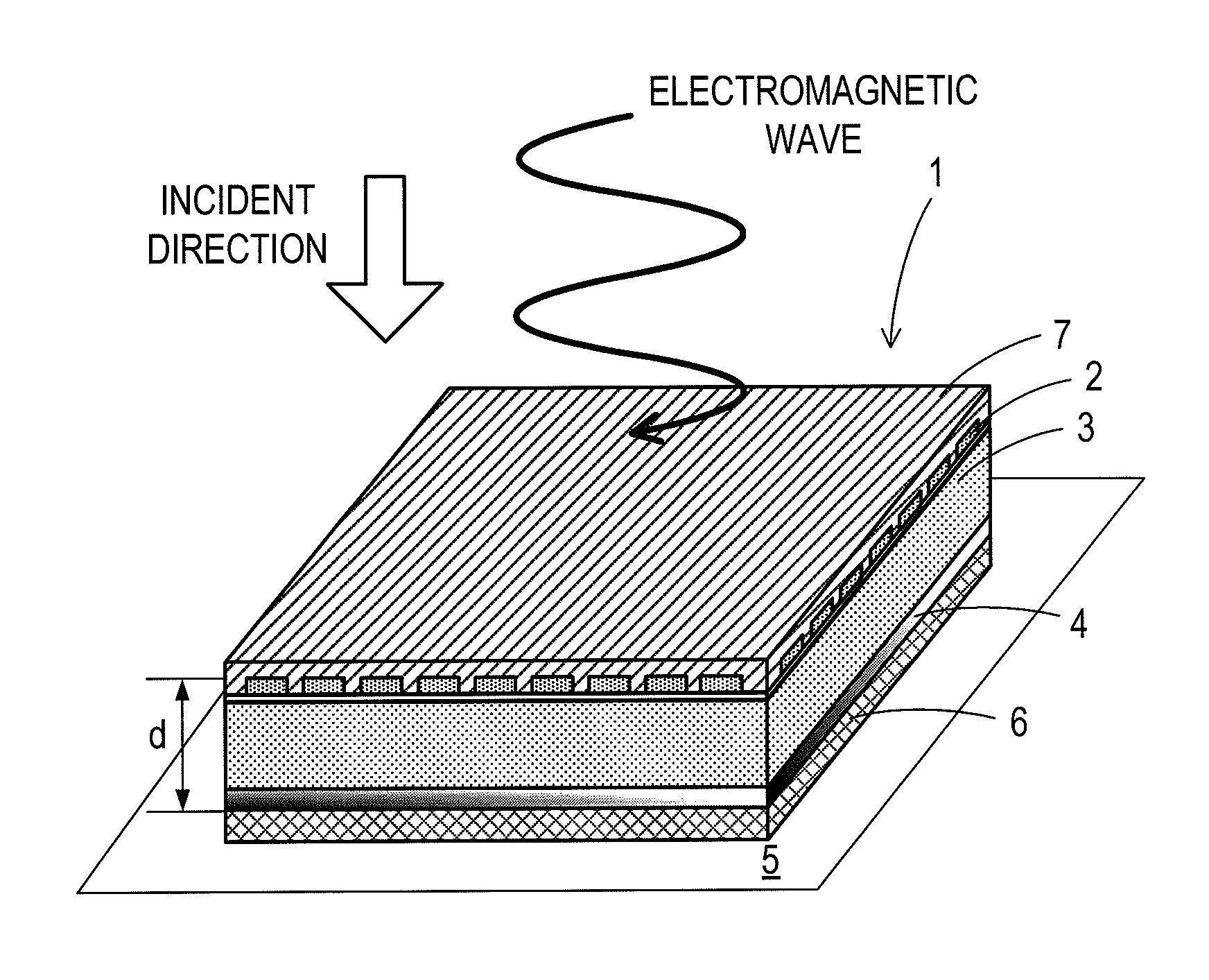
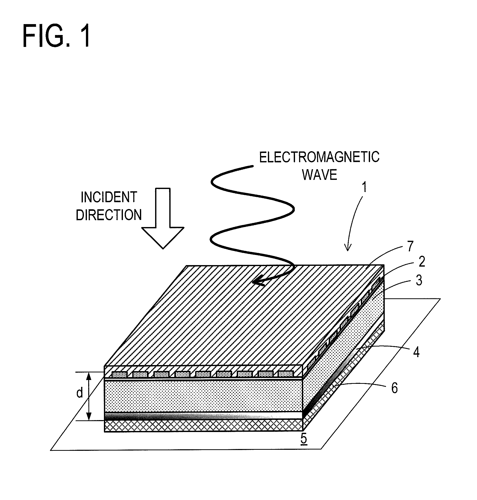
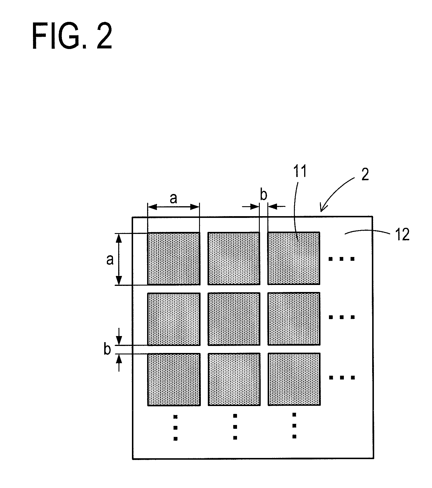
Electromagnetic wave absorber
a technology of electromagnetic waves and absorbers, applied in the field of electromagnetic waves absorbers, can solve the problems of unfavorable human body radiation of electromagnetic waves, erroneous operation of electronic components, and insignificant reduction in film thickness and weight of dielectric layers, etc., and achieve the effect of reducing film thickness and weigh
- Summary
- Abstract
- Description
- Claims
- Application Information
AI Technical Summary
Benefits of technology
Problems solved by technology
Method used
Image

Examples
embodiment
[0068]Embodiments of the present invention will be described hereinafter.
[0069]Firstly, manufacturing process of the electromagnetic wave absorber sheet 1 will be described.
[0070]First, dispersion treatment is carried out wherein 100 parts (by weight, similarly indicated hereinafter) of carbon black (BF-5AK manufactured by Chuetsu Graphite Works Co., Ltd.), 1 part of PGM (solvent, manufactured by Taiyou Kagaku Co., Ltd.) and 700 parts of Plysurf A212 (dispersant, manufactured by Dai-ichi Kogyo Seiyaku Co., Ltd.) are dispersed by a bead mill (APEX MILL manufactured by Kotobuki Industries Co., Ltd.). It is to be noted that the dispersion treatment conditions are the use of 6 kilograms of bead, 700 rotations per minute and processing speed of 0.1 hr / kg.
[0071]Next, the dispersion liquid obtained at the dispersion treatment is mixed with PMMA solution. The mixing ratio is 901 parts of the dispersion liquid, 500 parts of Delpet SR8500 (PMMA resin manufactured by Asahi Kasei Corporation), ...
PUM
 Abstract
Description
Claims
Application Information
 - R&D
- Intellectual Property
- Life Sciences
- Materials
- Tech Scout
- Unparalleled Data Quality
- Higher Quality Content
- 60% Fewer Hallucinations
Browse by: Latest US Patents, China's latest patents, Technical Efficacy Thesaurus, Application Domain, Technology Topic, Popular Technical Reports.
© 2025 PatSnap. All rights reserved.Legal|Privacy policy|Modern Slavery Act Transparency Statement|Sitemap|About US| Contact US: help@patsnap.com