Memory device

a memory device and memory technology, applied in semiconductor devices, semiconductor/solid-state device details, capacitors, etc., can solve the problems of short data retention period, loss of electric charge in capacitors, and difficulty in using capacitors in practice, and achieve the effect of extremely long data holding period

Inactive Publication Date: 2014-04-01
SEMICON ENERGY LAB CO LTD
View PDF178 Cites 17 Cited by
  • Summary
  • Abstract
  • Description
  • Claims
  • Application Information

AI Technical Summary

Benefits of technology

[0009]On the other hand, reduction in area occupied by a memory cell is required because capacity of a memory device becomes larger. The forementioned planar transistor and an RCAT which is a modification of the planar transistor can achieve higher integration density by reduction in width between wirings in a circuit; however, it is difficult to use them in practice because of technical problems. In addition, it is expected to reduce the occupied area by change in structure. The area of a memory cell is now larger than or equal to 8F2 (F: minimum feature size) or larger than or equal to 6F2. If a memory cell with a size of 4F2 can be formed, for example, the area occupied by a memory device can be reduced.
[0015]The semiconductor layer is preferably formed using a material with a band gap of greater than or equal to 2.5 eV and smaller than or equal to 4 eV. For example, an oxide semiconductor can be used. A transistor which includes the semiconductor layer for its channel formation region has an extremely low off-state current characteristic. Accordingly, the amount of electric charge flowing out from a capacitor and flowing therein is small, and a data holding period can be longer. In other words, refresh operations in a predetermined time can be reduced.
[0018]With use of an embodiment of the present invention, a memory device where an area occupied by a memory cell is small can be provided. Further, a memory device where an area occupied by a memory cell is small and a data holding period is extremely long can be provided.

Problems solved by technology

Thus, when data is read from conventional DRAM, electric charge in a capacitor is lost, so that another writing operation is necessary whenever data is read.
In addition, leakage current flows in a transistor included in a memory element and electric charge stored in the capacitor flows or an electric charge flows into the capacitor even if the transistor is not selected, whereby data retention period is short.
Thus, there has been a problem in that operation for writing data again in a predetermined cycle (refresh operation) is needed.
The forementioned planar transistor and an RCAT which is a modification of the planar transistor can achieve higher integration density by reduction in width between wirings in a circuit; however, it is difficult to use them in practice because of technical problems.

Method used


Image

  • Memory device
  • Memory device
  • Memory device

Examples


embodiment 1

(Embodiment 1)

[0040]In this embodiment, an example of a structure of a memory cell and a structure a memory device which are embodiments of the present invention will be described. Note that although a drawing illustrating part of a memory device is used for description in this embodiment, the number of bit lines and the number of word lines are not necessarily the ones defined in the description, and practitioners can set them freely.

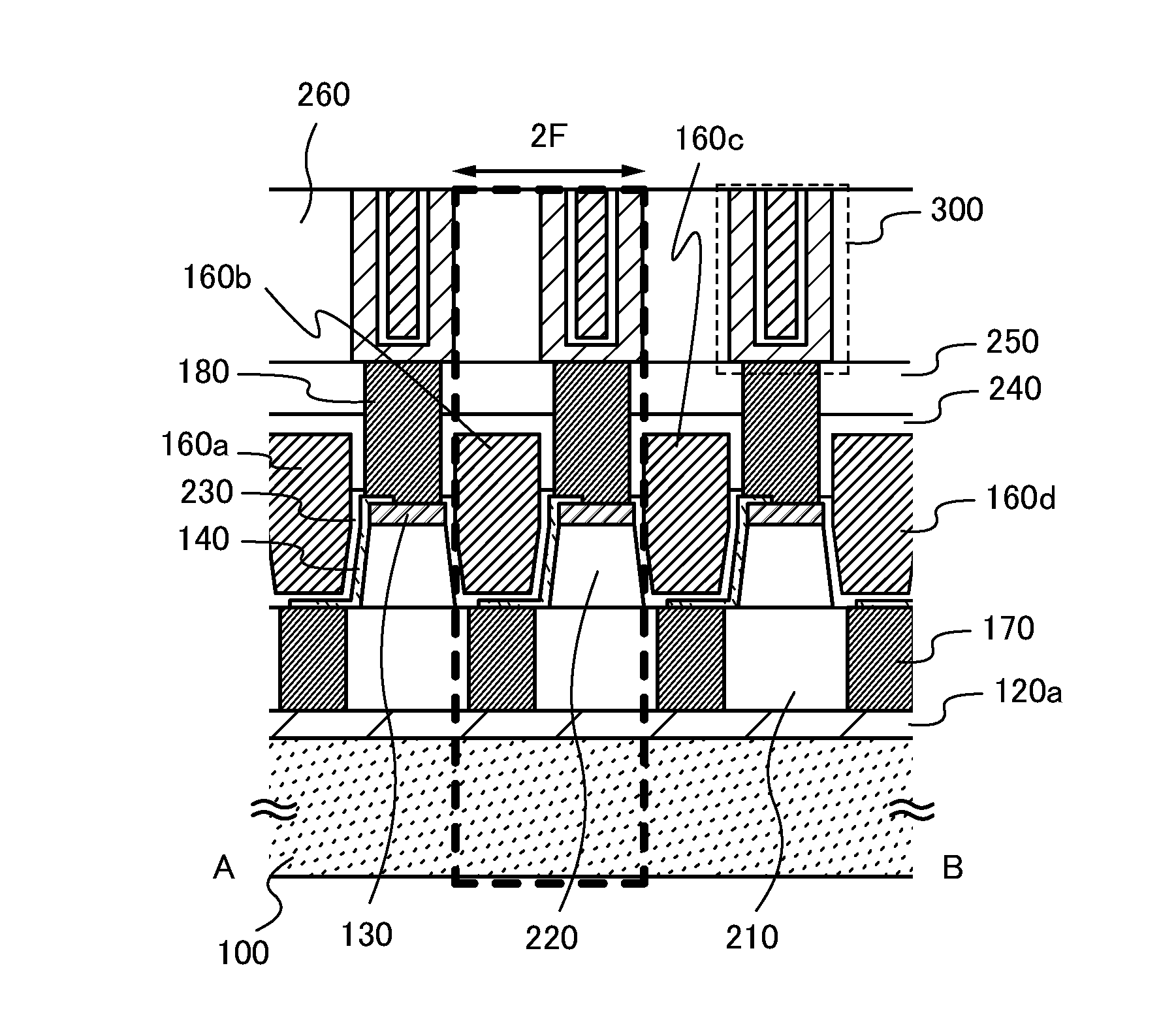
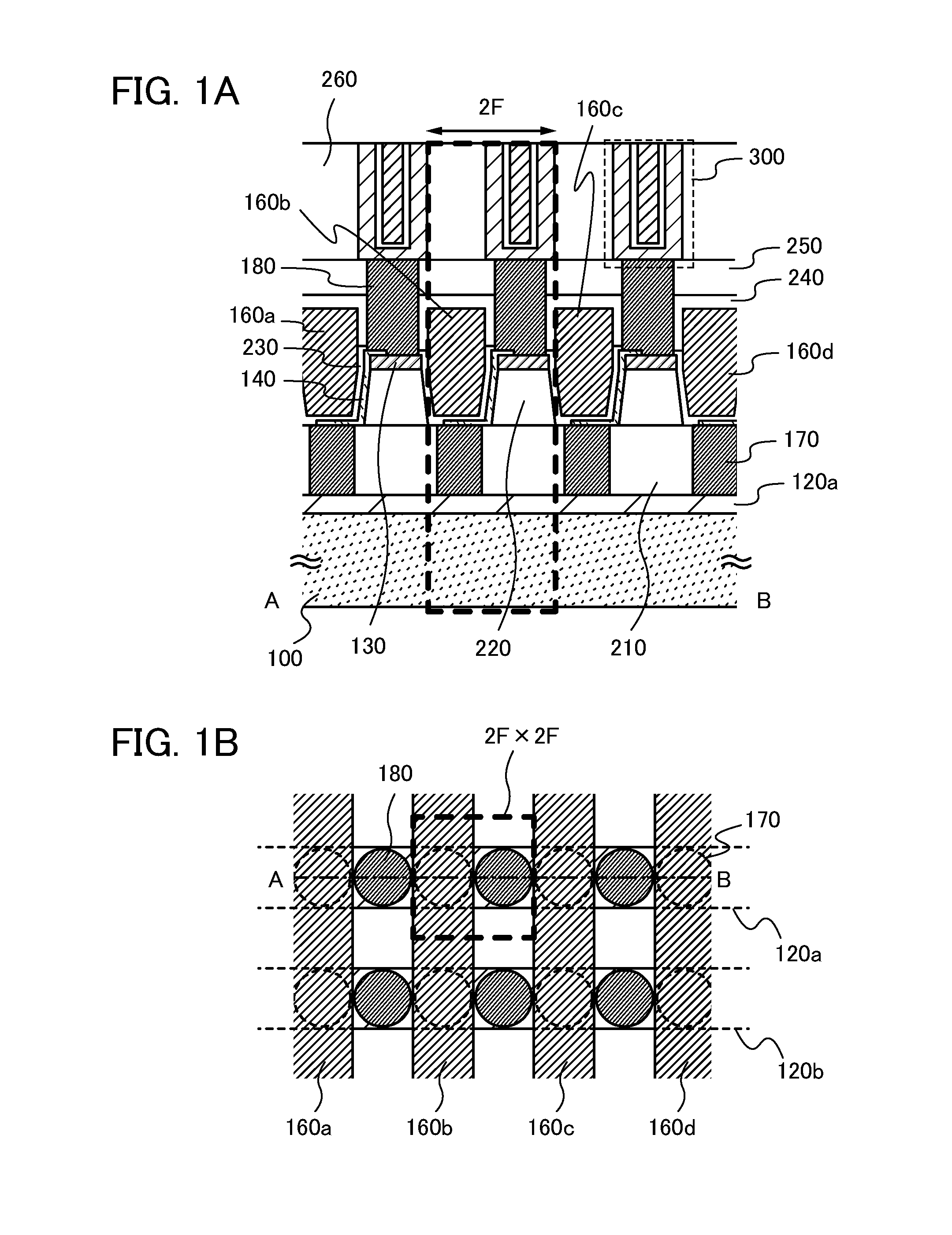
[0041]FIG. 1B illustrates part of a top view of a memory device in an embodiment of the present invention. A schematic structure is shown by a bit line 120a, a bit line 120b, a word line 160a, a word line 160b, a word line 160c, a word line 160d, a contact plug 170, and a contact plug 180. The other components are not shown for the sake of clarity.

[0042]FIG. 1A is a cross-sectional view of the memory device taken along line A-B in FIG. 1B. The memory device includes over a substrate 100, the bit line 120a; a first insulating layer 210 formed over the b...

embodiment 2

(Embodiment 2)

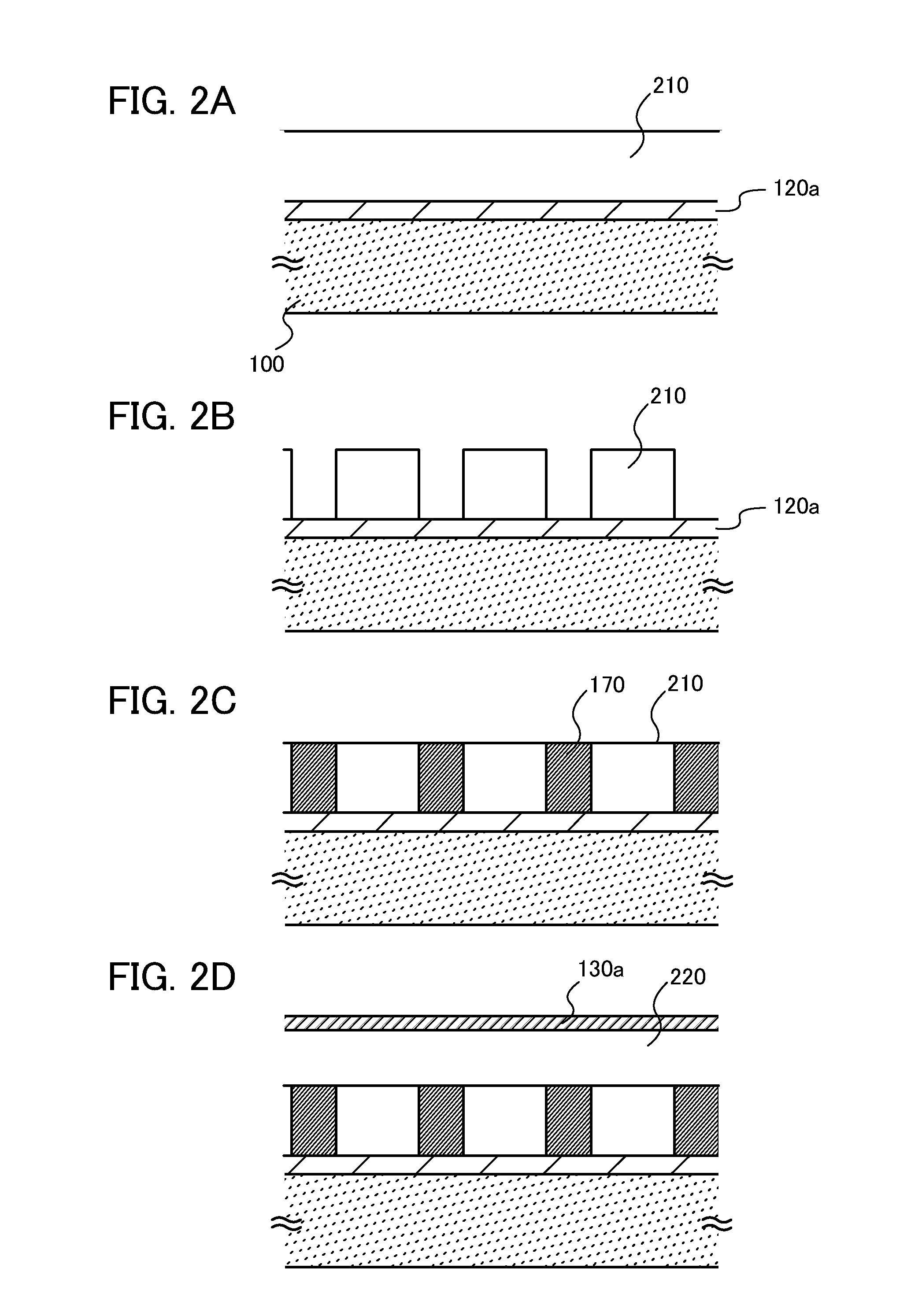
[0059]In this embodiment, a method for manufacturing the semiconductor memory device described in Embodiment 1 as an example is described. Note that the drawing used for the description is a cross-sectional view taken along line A-B in FIG. 1B.

[0060]First, the bit line 120a is formed over the substrate 100, and the first insulating layer 210 is formed over the substrate and the bit line (see FIG. 2A).

[0061]Although there is no particular limitation on a material which can be used as the substrate 100, it is necessary that the material have at least heat resistance high enough to withstand heat treatment to be performed later. For example, the substrate 100 may be a glass substrate, a quartz substrate, a semiconductor substrate, a ceramic substrate, or the like. When the temperature of the heat treatment performed later is high, a substrate having a strain point of 730° C. or higher is preferably used as the glass substrate. Here, a glass substrate is used.

[0062]Note th...

embodiment 3

(Embodiment 3)

[0092]In this embodiment, an example of a memory device in which memory cells described in Embodiments 1 and 2 are stacked over a substrate with which a semiconductor circuit is formed will be described.

[0093]FIG. 6 is a cross-sectional view of a memory device where a memory cell portion is stacked over a semiconductor substrate where a driver circuit portion is formed. In the memory device, a driver circuit portion 420 for driving a memory cell such as a sense amplifier or a decoder is formed on a single crystal semiconductor substrate 400 by a known technique for forming a semiconductor integrated circuit. A memory cell portion 440 can be manufactured by referring to Embodiment 2.

[0094]A bit line connected to the cell transistor is electrically connected to the driver circuit portion 420 provided in a lower layer through a contact plug or the like. Accordingly, a potential signal output from the driver circuit portion 420 is input to each cell transistor through a co...


PUM


Abstract

It is an object to provide a memory device where an area occupied by a memory cell is small, and moreover, a memory device where an area occupied by a memory cell is small and a data holding period is long. A memory device includes a bit line, a capacitor, a first insulating layer provided over the bit line and including a groove portion, a semiconductor layer, a second insulating layer in contact with the semiconductor layer, and a word line in contact with the second insulating layer. Part of the semiconductor layer is electrically connected to the bit line in a bottom portion of the groove portion, and another part of the semiconductor layer is electrically connected to one electrode of the capacitor in a top surface of the first insulating layer.

Description

BACKGROUND OF THE INVENTION[0001]1. Field of the Invention[0002]The present invention relates to a memory device using semiconductor characteristics.[0003]2. Description of the Related Art[0004]Dynamic random access memory (DRAM) with a memory cell including one capacitor and one transistor (also referred to as a cell transistor) is widely used as a typical memory device.[0005]Note that in this specification, a memory cell indicates a circuit configuration needed for holding a minimum unit of data, and a memory device indicates a semiconductor device including at least integrated memory cells.[0006]A planar transistor has been conventionally used to form a DRAM; however, a method using a recessed channel array transistor (RCAT) in which a gate is arranged three-dimensionally so as to prevent leakage current due to a short-channel effect caused by miniaturization of a circuit is now employed (see Non-Patent Document 1).REFERENCE[0007][Non-Patent Document] K. Kim, “Technology for sub-...

Claims


Application Information

Patent Timeline
Patent Type & Authority Patents(United States)
IPC IPC(8): H01L23/48H01L27/108H01L29/94H01L23/52H01L29/12H01L29/10H01L29/40
CPCH01L27/10808H01L28/91H01L27/10876H01L27/1203H01L27/10814H01L21/84H10B12/31H10B12/315H10B12/053H10B99/00H10B12/00
Inventor KATO, KIYOSHISAITO, TOSHIHIKO
Owner SEMICON ENERGY LAB CO LTD
Why Eureka
Try Eureka