Method for manufacturing bonded wafer

a technology of bonded wafers and manufacturing methods, applied in the direction of basic electric elements, electrical apparatus, semiconductor devices, etc., can solve the problems of easy damage, low physical resistance, and thin thickness of silicon, and achieve high bonding strength, suppress the diffusion of ion-implanted hydrogen atoms, and high quality

Active Publication Date: 2014-04-15
SHIN-ETSU HANDOTAI CO LTD
View PDF27 Cites 0 Cited by
  • Summary
  • Abstract
  • Description
  • Claims
  • Application Information

AI Technical Summary

Benefits of technology

[0012]The present invention was accomplished in view of the above-explained circumstances, and its object is to provide a method for manufacturing a high quality bonded wafer by forming a high bonding strength state at a lower temperature than the temperature at which the delamination is caused and reducing the generation of the defects in the delamination process, in the manufacture of the bonded wafer by the Smart Cut method (registered trademark).
[0014]In this manner, when the pre-annealing is performed at a temperature of less than 500° C. at least by the heat treatment at the first temperature and the subsequent heat treatment at the second temperature higher than the first temperature and thereafter the delamination heat treatment is performed at the temperature of 500° C. or more, the bonding strength can be enhanced at a lower temperature than the temperature at which the delamination is caused, the voids and the blisters can be thereby reduced, and the bonded wafer having few defects can be consequently manufactured.
[0018]In this manner, when the second temperature in the pre-annealing is nearly 350° C., the diffusion of ion-implanted hydrogen atoms can be suppressed, and the delamination can be fully performed in the subsequent delamination heat treatment.
[0019]With the method for manufacturing a bonded wafer according to the present invention, a high quality bonded wafer (including an SOI wafer and a directly bonded wafer) can be manufactured by forming a high bonding strength state at a lower temperature than the temperature at which the delamination is caused and reducing the generation of the defects generated in the delamination process, such as the voids and the blisters.

Problems solved by technology

After the delamination, the thickness of silicon is thin, and the physical resistance is therefore low.
In case of low bonding strength, for example, the SOI layer flakes off and is easily damaged, and the defects thereof are thus generated.
However, even when the pre-annealing is performed before the delamination heat treatment as described above, an incidence of the SOI layer defects, such as blisters (portions where the SOI layer is not bonded to the base wafer) or voids (portions where the SOI layer is not formed), cannot be sufficiently reduced in some cases.

Method used


Image

  • Method for manufacturing bonded wafer
  • Method for manufacturing bonded wafer

Examples


example 1

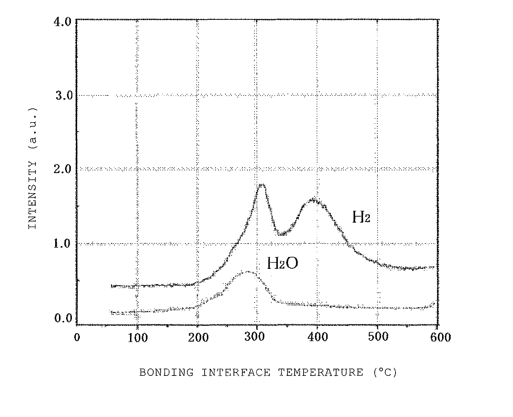
[0039]There were prepared 300 silicon single crystal wafers having a diameter of 300 mm. The prepared wafers were divided into the bond wafers and the base wafers. The thermal oxide film having a thickness of 150 nm was formed on the surface of each of the bond wafers. Then, hydrogen ions were implanted inside each of the bond wafers through the thermal oxide film (an implantation energy of 46 keV, and a dose amount of 5×10¹⁶ / cm2).

[0040]The bond wafers were thereafter bonded to the base wafers at a room temperature each, and the heat treatment was performed to delaminate each of the bond wafers. At this point, the heat treatment conditions included the pre-annealing having the heat treatments at the first temperature and second temperature. The heat treatment at the first temperature in the pre-annealing was performed at a temperature of 200° C. for 4 hours, and the heat treatment at the second temperature in the pre-annealing was performed at a temperature of 350° C. for 2 hours. T...

example 2

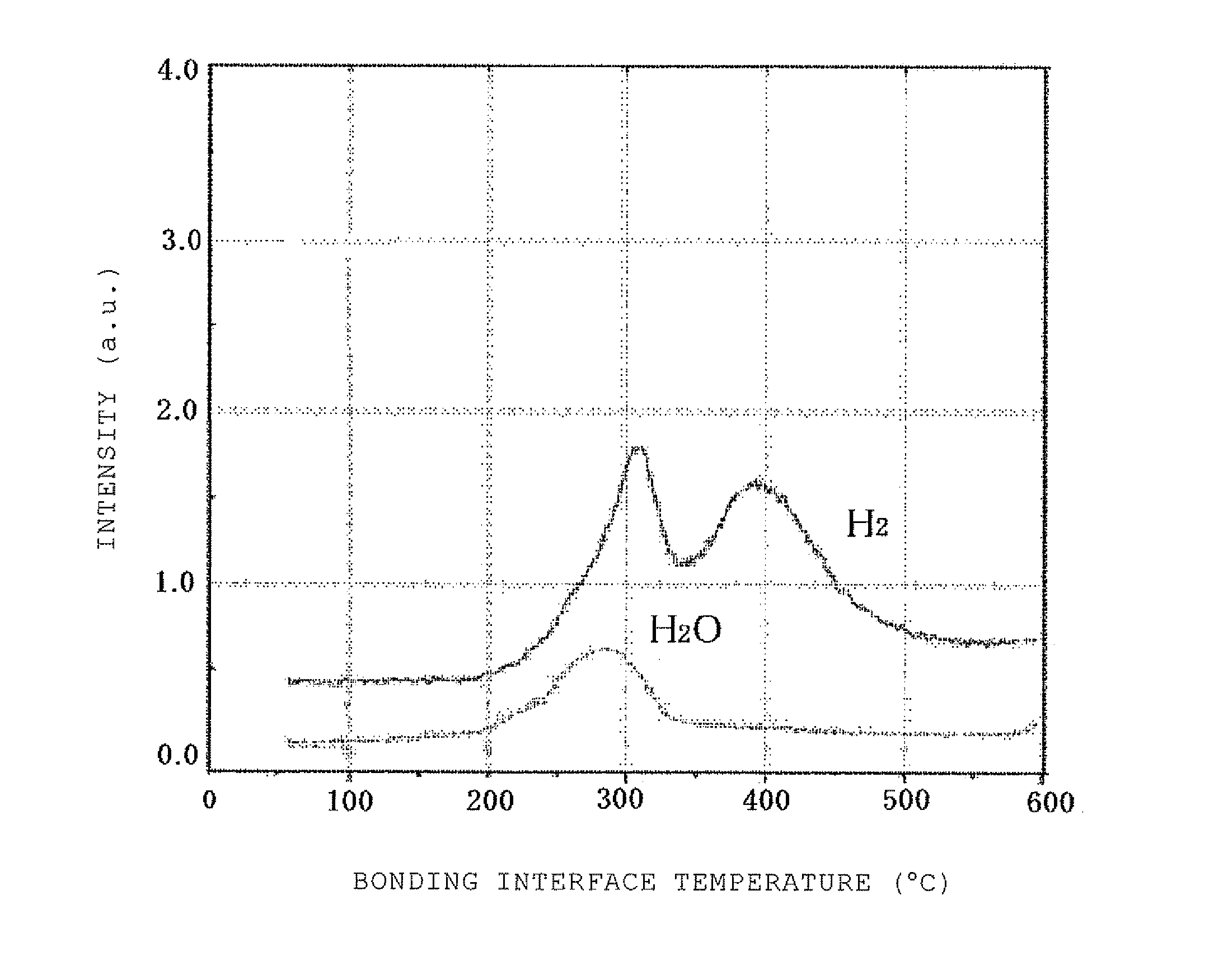
[0045]There were prepared 300 silicon single crystal wafers having a diameter of 300 mm. The prepared wafers were divided into the bond wafers and the base wafers. The thermal oxide film having a thickness of 20 nm was formed on the surface of each of the bond wafers. Then, hydrogen ions were implanted inside each of the bond wafers through the thermal oxide film (an implantation energy of 35 keV, and a dose amount of 5×10¹⁶ / cm2).

[0046]The bonding interface of the bond wafers were thereafter subjected to nitrogen plasma treatment for enhancing the bonding strength at a room temperature. Then, the bond wafers were bonded to the base wafers at a room temperature each, and the heat treatment was performed to delaminate each of the bond wafers. At this point, the heat treatment conditions included the pre-annealing having the heat treatments at the first temperature and second temperature. The heat treatment at the first temperature in the pre-annealing was performed at a temperature of...


PUM

PropertyMeasurementUnit
temperatureaaaaaaaaaa

Abstract

The present invention is a method for manufacturing a bonded wafer including at least the steps of: forming an ion-implanted layer inside a bond wafer; bringing the ion-implanted surface of the bond wafer into close contact with a surface of a base wafer directly or through a silicon oxide film; and performing heat treatment for delaminating the bond wafer at the ion-implanted layer, wherein the heat treatment step for delaminating includes performing a pre-annealing at a temperature of less than 500° C. and thereafter performing a delamination heat treatment at a temperature of 500° C. or more, and the pre-annealing is performed at least by a heat treatment at a first temperature and a subsequent heat treatment at a second temperature higher than the first temperature. As a result, there is provided a method for manufacturing a bonded wafer having high quality, for example, mainly the reduction of defects, by forming a high bonding strength state at a lower temperature than the temperature at which the delamination is caused, in the manufacture of the bonded wafer by the Smart Cut method (registered trademark).

Description

TECHNICAL FIELD[0001]The present invention relates to a method for manufacturing a bonded wafer by using a Smart Cut method (registered trademark), and typically to a method for manufacturing an SOI wafer or a directly bonded wafer by bringing a wafer as a supporting substrate into close contact with a silicon wafer into which hydrogen ions and the like are implanted and thereafter delaminating it.BACKGROUND ART[0002]As the generation of devices advances, the goal of a higher performance trend cannot be achieved only by a scaling effect with a conventional bulk silicon wafer, and a new device structure is accordingly needed. An SOI wafer has been paid attention to as a starting raw material. The SOI wafer is manufactured by a bonding method (thinning a thickness by grinding and polishing), a SIMOX method, or a Smart Cut method (registered trademark: thinning a thickness by an ion implantation delamination). The SOI wafer has been mainly used which is manufactured by using the Smart ...

Claims


Application Information

Patent Timeline
Patent Type & Authority Patents(United States)
IPC IPC(8): H01L21/30
CPCH01L21/76254H01L21/20H01L27/12
Inventor ISHIZUKA, TOHRUKOBAYASHI, NORIHIRONOTO, NOBUHIKO
Owner SHIN-ETSU HANDOTAI CO LTD
Why Eureka
Try Eureka