

Method, system, and program product for interactive checking for double pattern lithography violations
a technology of double pattern lithography and interactive checking, applied in the field of electronic design automation, can solve the problems of inability to project an accurate image of increasingly smaller features onto the wafer, conventional tools do not have the ability to interactively track, and non-standard geometries on a single layer normally cannot be printed on silicon
- Summary
- Abstract
- Description
- Claims
- Application Information
AI Technical Summary
Benefits of technology
Problems solved by technology
Method used
Image

Examples
Embodiment Construction
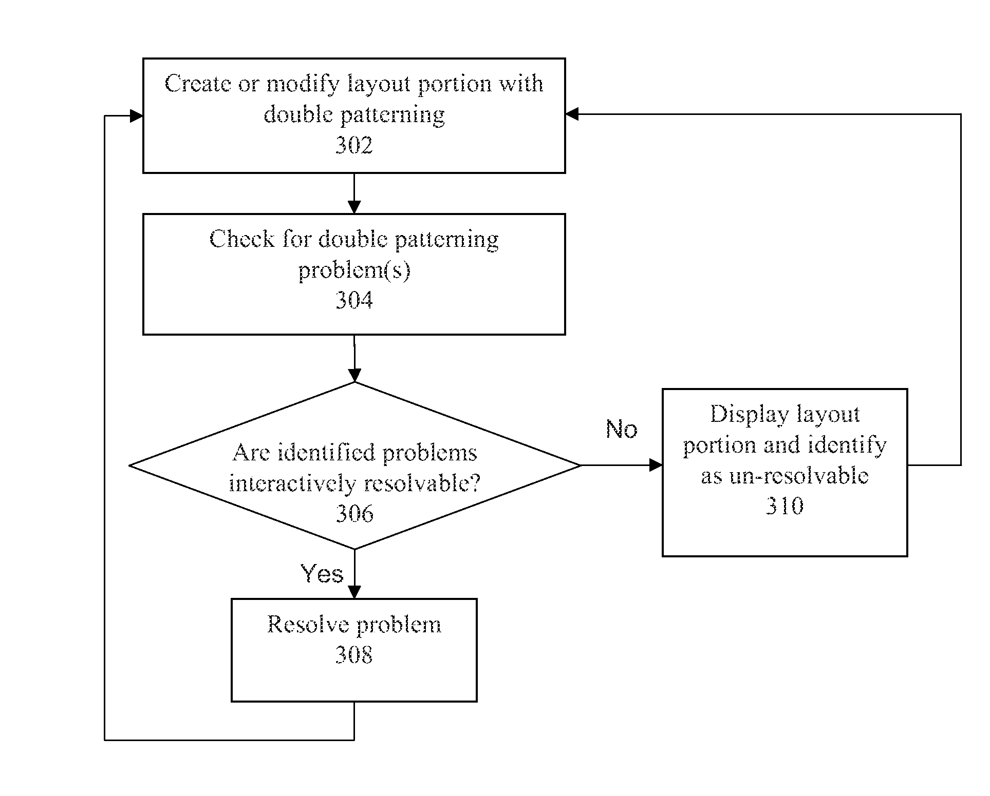
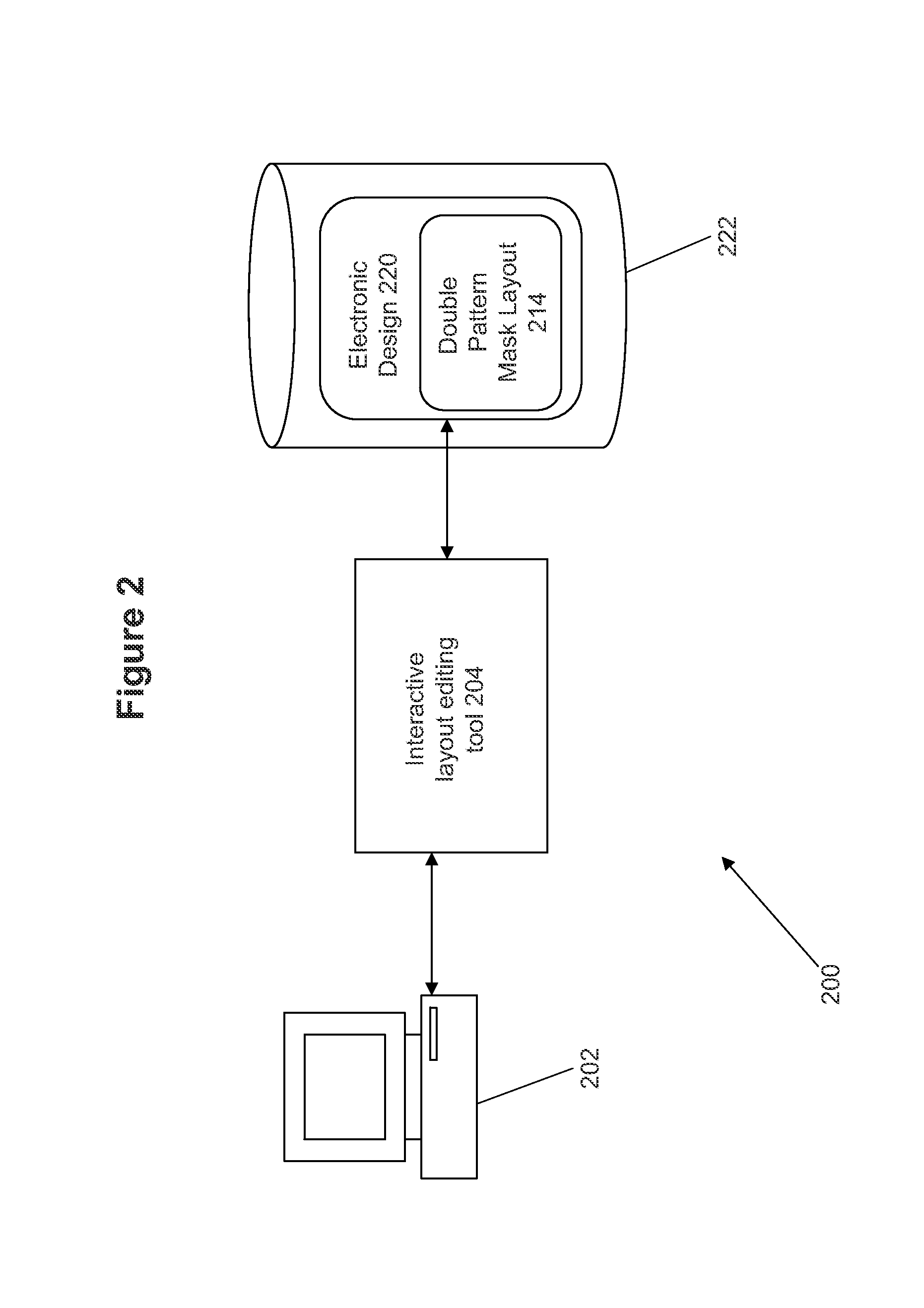
[0022]Embodiments of the present invention provide a method, apparatus, and program product for performing interactive layout editing to address double patterning approaches to implement lithography of electronic designs. A feature of an embodiment of the present invention is to perform spatial query around the shape(s) being created during editing with the distance of allowed spacing in a single mask. If a design error is encountered, corrective editing may occur to correct the error. The present approach can be configured to allow the error detection and corrective actions to be performed interactively.
[0023]To explain the problem being addressed by embodiments of the invention, consider that the minimum feature size that a projection system can print can be expressed by:
[0024]CD=k1λNA
where CD, critical dimension, is the minimum feature size; k1 is a dimensionless coefficient of process-related factors; A is the wavelength of light used; and NA is the numerical aperture of the pr...
PUM
 Abstract
Description
Claims
Application Information