Semiconductor memory device

a memory device and semiconductor technology, applied in semiconductor devices, capacitors, instruments, etc., can solve the problems of data loss, increase in power consumption of semiconductor memory devices, and transistors that do not function as switching elements, etc., to reduce the price per storage capacity of semiconductor devices, and achieve high degree of integration

Inactive Publication Date: 2014-07-08
SEMICON ENERGY LAB CO LTD
View PDF145 Cites 15 Cited by
  • Summary
  • Abstract
  • Description
  • Claims
  • Application Information

AI Technical Summary

Benefits of technology

[0009]The sizes of elements (e.g., a transistor and a capacitor) included in a semiconductor memory device need to be reduced in order to increase the degree of integration of the semiconductor memory device. When the size of a transistor is reduced in accordance with the scaling law, influence of a short-channel effect cannot be avoided, for example, in the case where the channel length is 100 nm or less, and punch-through leakage current easily flows, which causes a problem that the transistor does not function as a switching element.
[0010]An object of one embodiment of the present invention is to increase data retention time of a semiconductor memory device while increasing the degree of integration of the semiconductor memory device.
[0016]Note that off-state current of a transistor can be reduced by using an oxide semiconductor film in a channel region of a transistor.
[0020]By applying one embodiment of the present invention, a semiconductor memory device which holds data for a long period and has a high degree of integration can be provided.
[0021]Further, a semiconductor memory device with a high degree of integration can be manufactured; thus, the price per storage capacity of the semiconductor device can be reduced.
[0022]By providing a channel region in contact with a groove provided in an insulating film, data retention time of a semiconductor memory device can be increased while increasing the degree of integration of the semiconductor memory device.

Problems solved by technology

However, a conventional semiconductor memory device has a problem that data is lost due to leakage of electric charge after the data is written to a memory transistor.
Therefore, refresh operation in which data is written periodically is needed, which results in an increase in power consumption of the semiconductor memory device.
When the size of a transistor is reduced in accordance with the scaling law, influence of a short-channel effect cannot be avoided, for example, in the case where the channel length is 100 nm or less, and punch-through leakage current easily flows, which causes a problem that the transistor does not function as a switching element.

Method used


Image

  • Semiconductor memory device
  • Semiconductor memory device
  • Semiconductor memory device

Examples


embodiment 1

(Embodiment 1)

[0032]In this embodiment, structures of transistors and a capacitor which are included in a nonvolatile memory that is a semiconductor memory device to which one embodiment of the present invention is applied, a circuit configuration, and a manufacturing method of the nonvolatile memory will be described with reference to FIGS. 1A to 1D, FIGS. 2A to 2C, and FIGS. 3A to 3E.

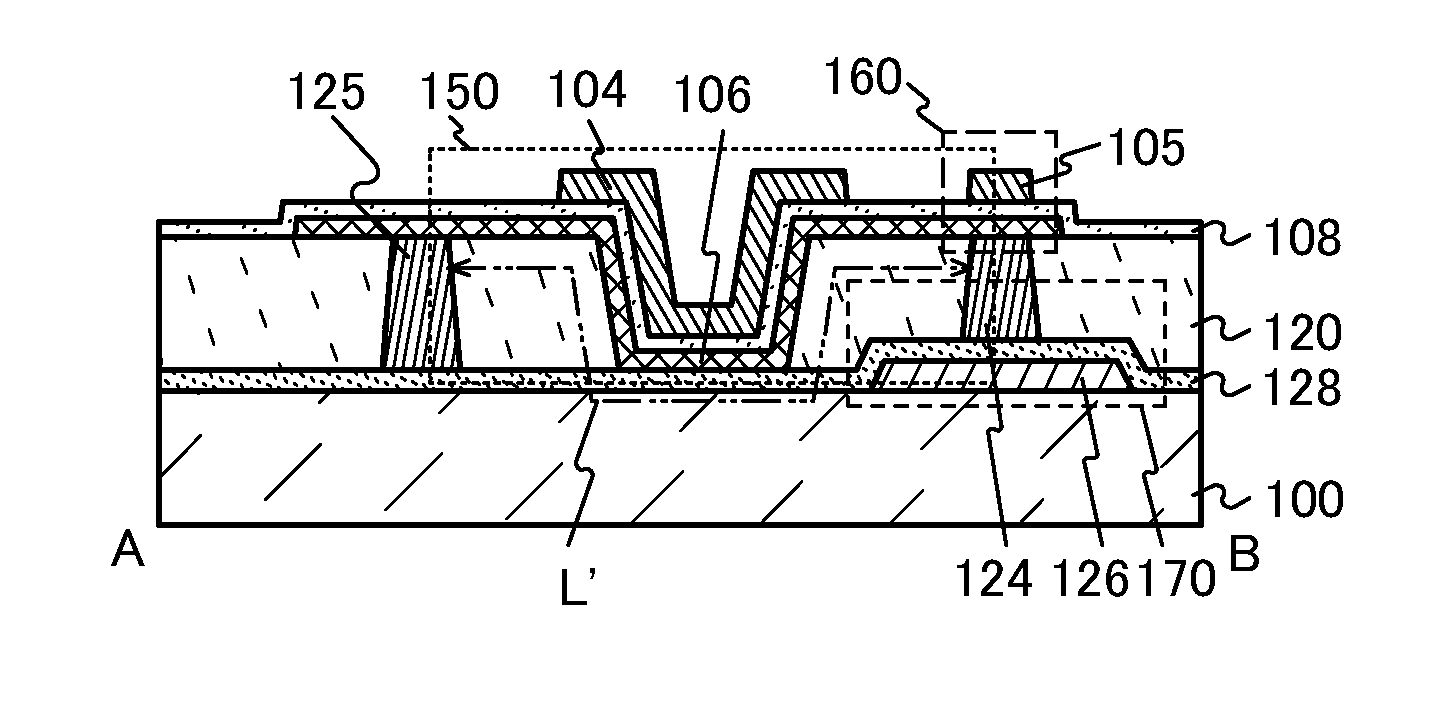
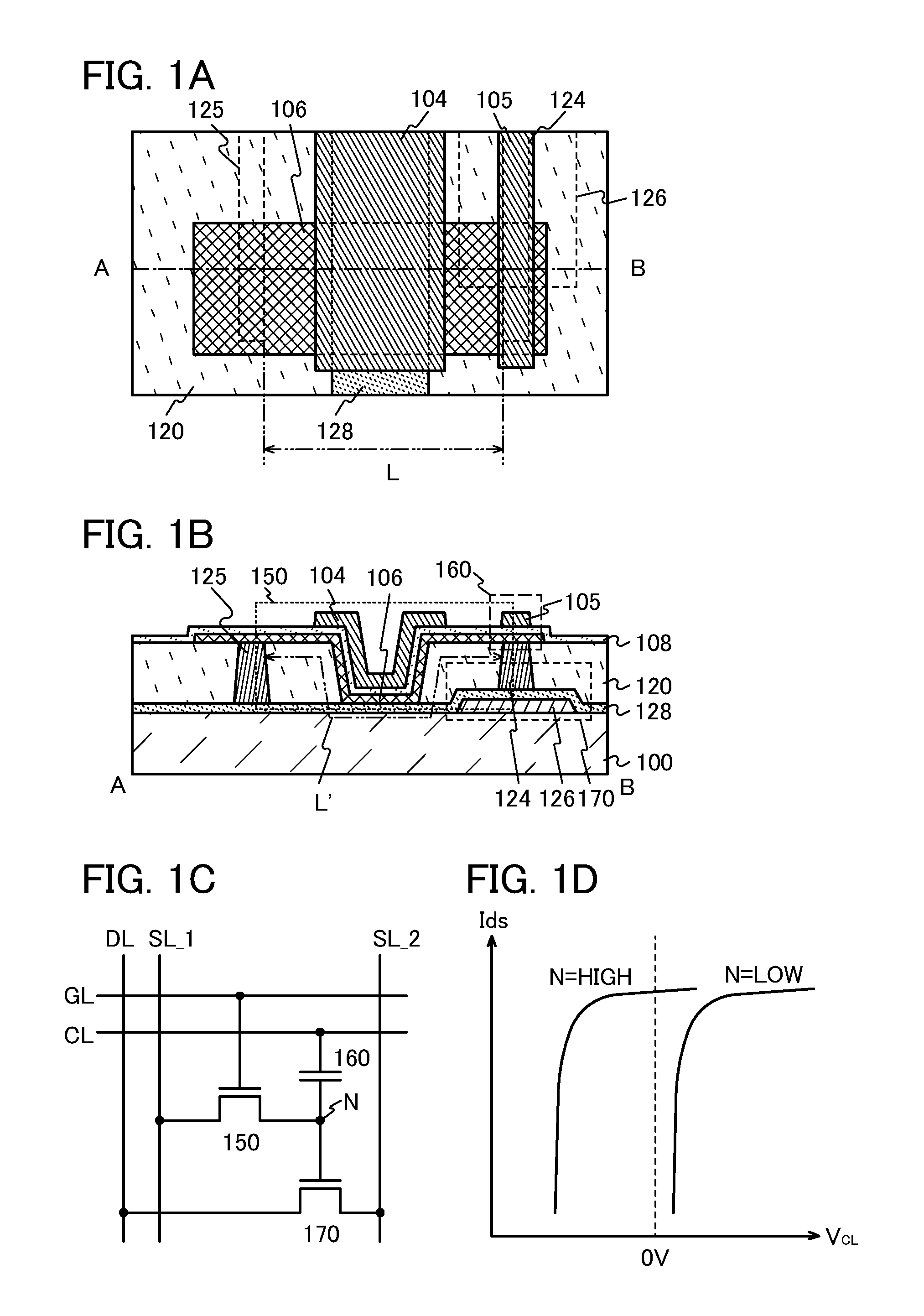
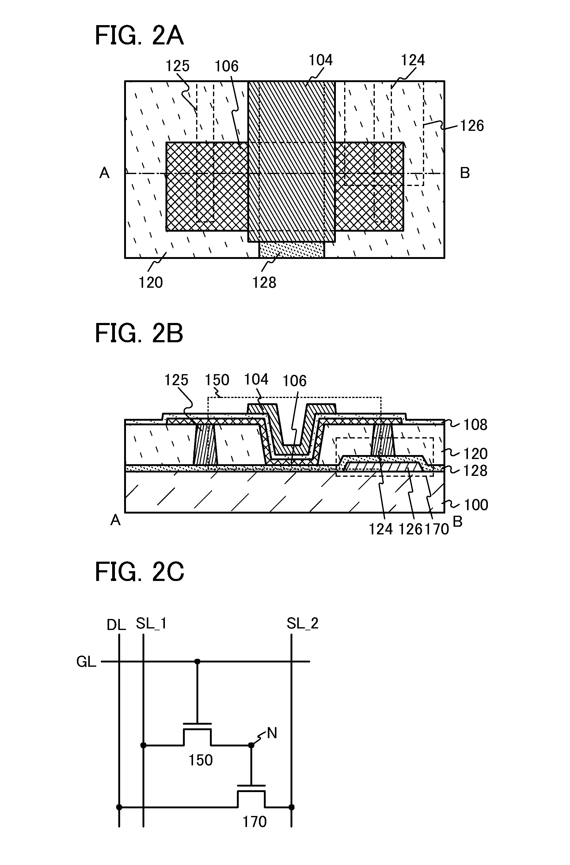
[0033]FIG. 1A is a top view of a nonvolatile memory that is a semiconductor memory device. FIG. 1B is a cross section A-B along a dashed-dotted line A-B in FIG. 1A. Note that an insulating film 108 is omitted in FIG. 1A for simplicity.

[0034]FIG. 1C illustrates a circuit configuration of the nonvolatile memory. The nonvolatile memory includes a transistor 150 with extremely small off-state current, a gate line GL connected to a gate of the transistor 150, a source line SL_1 connected to a source of the transistor 150, a transistor 170, a source line SL_2 connected to a source of the transistor 170, a d...

embodiment 2

(Embodiment 2)

[0101]In this embodiment, examples of electronic devices to which Embodiment 1 is applied will be described.

[0102]FIG. 4A illustrates a portable information terminal The portable information terminal includes a housing 9300, a button 9301, a microphone 9302, a display portion 9303, a speaker 9304, and a camera 9305, and has a function as a mobile phone. One embodiment of the present invention can be applied to a memory module inside the portable information terminal

[0103]FIG. 4B illustrates a digital still camera. The digital still camera includes a housing 9320, a button 9321, a microphone 9322, and a display portion 9323. One embodiment of the present invention can be applied to a memory module inside the digital still camera.

[0104]The use of one embodiment of the present invention makes it possible to reduce power consumption of electronic devices and to reduce the costs of the electronic devices.

[0105]This embodiment can be implemented in appropriate combination wi...


PUM


Abstract

A semiconductor memory device includes a semiconductor film; a first gate insulating film covering the semiconductor film; a first gate electrode provided over the semiconductor film with the first gate insulating film interposed therebetween; a first conductive film which is provided over the first gate insulating film; an insulating film which is provided over the first gate insulating film, exposes top surfaces of the first gate electrode and the first conductive film, and has a groove portion between the first gate electrode and the first conductive film; an oxide semiconductor film which is provided over the insulating film and is in contact with the first gate electrode, the first conductive film, and the groove portion; a second gate insulating film covering the oxide semiconductor film; and a second gate electrode provided over the oxide semiconductor film and the groove portion with the second gate insulating film interposed therebetween.

Description

BACKGROUND OF THE INVENTION[0001]1. Field of the Invention[0002]The present invention relates to a semiconductor memory device which includes a circuit including a semiconductor element such as a transistor.[0003]2. Description of the Related Art[0004]Semiconductor memory devices including memory circuits capable of writing, reading, and erasing data have been developed.[0005]As examples of the semiconductor memory device, a semiconductor memory device including a transistor that is a memory element (also referred to as memory transistor) or an element formed using a ferroelectric material, and the like are given (see Patent Document 1 and Patent Document 2).REFERENCE[0006][Patent Document 1] Japanese Published Patent Application No. S57-105889[0007][Patent Document 2] Japanese Published Patent Application No. H06-196647SUMMARY OF THE INVENTION[0008]However, a conventional semiconductor memory device has a problem that data is lost due to leakage of electric charge after the data is...

Claims


Application Information

Patent Timeline
Patent Type & Authority Patents(United States)
IPC IPC(8): H01L29/76H01L29/12
CPCH01L28/40H01L27/1156G11C16/0433H10B41/70H01L29/78645H01L29/7869
Inventor NODA, KOSEI
Owner SEMICON ENERGY LAB CO LTD
Why Eureka
Try Eureka