Method for manufacturing semiconductor device
a manufacturing method and semiconductor technology, applied in semiconductor devices, semiconductor/solid-state device details, electrical devices, etc., can solve the problems of difficult exposure from the front face, channel thickness, and inability to apply double-sided aligners to the fabrication of transistors requiring alignment of sub-micron scale or smaller, etc., to achieve easy manufacturing of semiconductor devices, high on characteristics, and high off characteristics. , the effect of reducing the risk of failur
- Summary
- Abstract
- Description
- Claims
- Application Information
AI Technical Summary
Benefits of technology
Problems solved by technology
Method used
Image


Examples
first embodiment
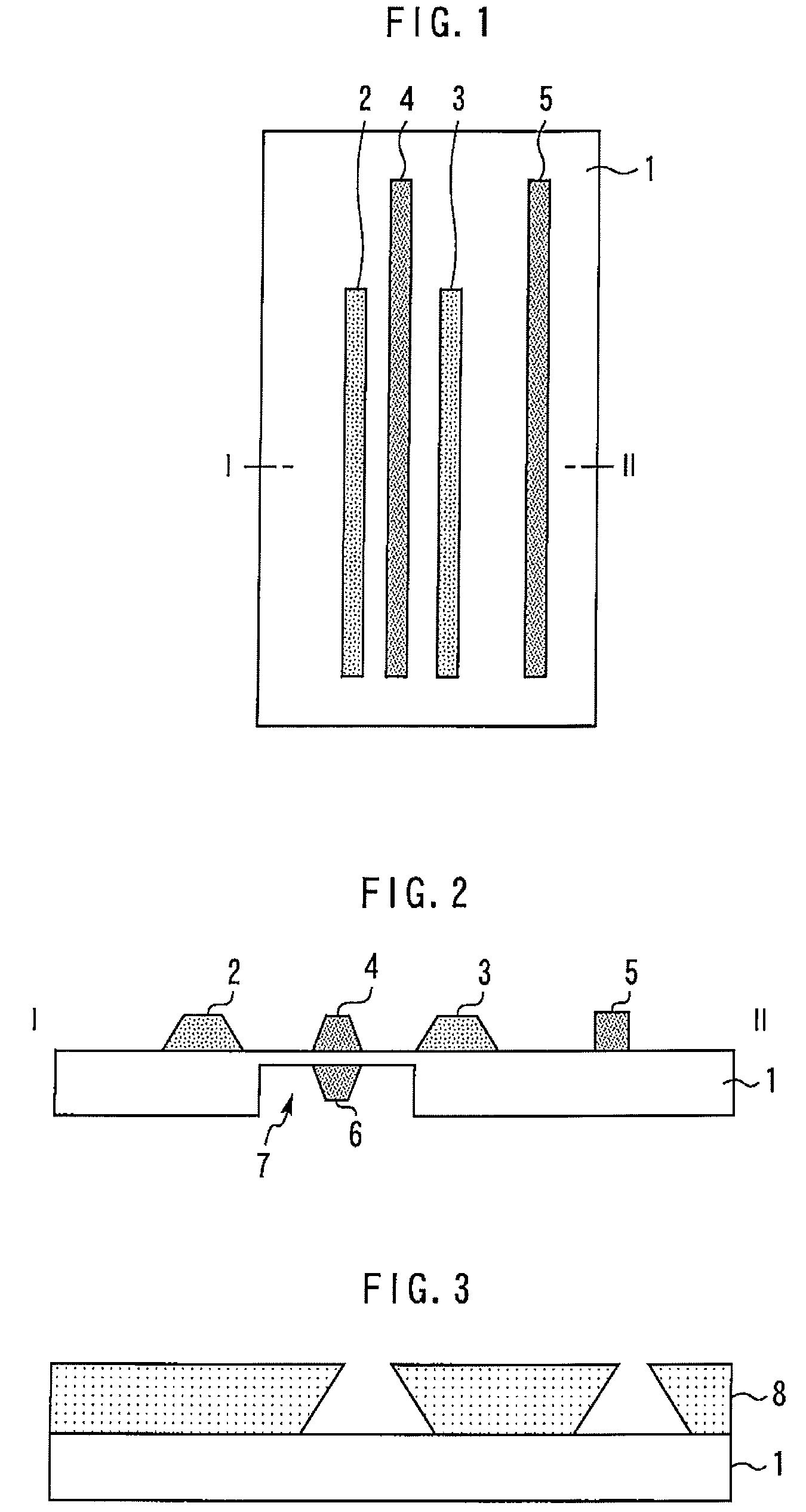
[0019]FIG. 1 is a top view showing a semiconductor device according to a first embodiment of the present invention. FIG. 2 is a sectional view taken along line I-II in FIG. 1. The semiconductor substrate 1 is transparent to visible light, and is formed of a wide-gap semiconductor, such as SiC and GaN.
[0020]A source electrode 2 and a drain electrode 3 are formed on the front face of the semiconductor substrate 1, and the front-side gate electrode 4 is formed in between. An aligning mark 5 is formed on the region of the front face of the semiconductor substrate 1 other than the region between the source electrode 2 and the drain electrode 3. A back-side gate electrode 6 is formed on the back face of the semiconductor substrate 1 opposite the front-side gate electrode 4. The back-side gate electrode 6 is placed in a recess 7 formed on the back face of the semiconductor substrate 1.
[0021]The source electrode 2 and the drain electrode 3 are formed of, for example, Au. The front-side gate...
second embodiment
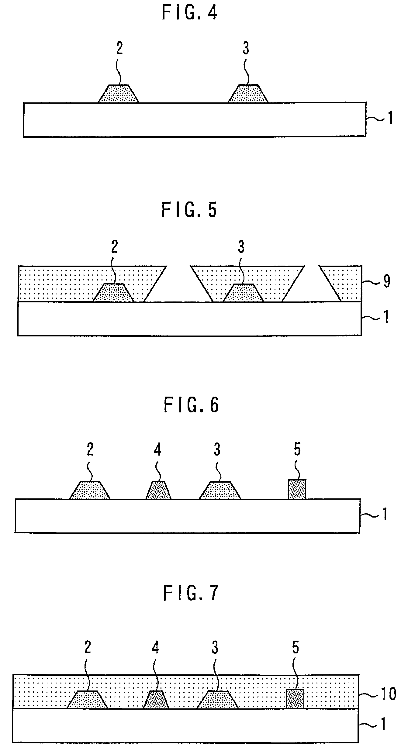
[0037]FIG. 11 is a sectional view showing a semiconductor device according to a second embodiment of the present invention. In the present embodiment, the front-side gate electrode 4 is T-shaped. The gate length of the front-side gate electrode 4 is identical to the gate length of the back-side gate electrode 6. Other components and methods for fabrication are identical to those in the first embodiment.
[0038]When the front-side gate electrode 4 is T-shaped, according to conventional methods wherein the resist applied to the back face is exposed from the front face using the front-side gate electrode 4 as the mask, the gate length of the back-side gate electrode 6 becomes longer than the gate length of the front-side gate electrode 4. On the other hand, in the present embodiment, since exposure is performed through the back face when the back-side gate electrode 6 is formed, the gate length of the front-side gate electrode 4 can be identical to the gate length of the back-side gate e...
third embodiment
[0039]FIG. 12 is a sectional view showing a semiconductor device according to a third embodiment of the present invention. In the present embodiment, an insulator 13 is filled in the recess 7 to coat the back-side gate electrode 6 with the insulator 13. The insulator 13 is formed of, for example, SiN. Thereafter, a metal 14 for die bonding electrically connected to the source electrode 2 on the back face of the semiconductor substrate 1 is formed. Other components and fabricating methods are identical to those in the first embodiment. By thus coating the back-side gate electrode 6 with the insulator 13, short-circuiting between the back-side gate electrode 6 and the source electrode 2 can be prevented.
PUM
 Abstract
Description
Claims
Application Information
 - R&D
- Intellectual Property
- Life Sciences
- Materials
- Tech Scout
- Unparalleled Data Quality
- Higher Quality Content
- 60% Fewer Hallucinations
Browse by: Latest US Patents, China's latest patents, Technical Efficacy Thesaurus, Application Domain, Technology Topic, Popular Technical Reports.
© 2025 PatSnap. All rights reserved.Legal|Privacy policy|Modern Slavery Act Transparency Statement|Sitemap|About US| Contact US: help@patsnap.com