Film forming method, semiconductor device, manufacturing method thereof and substrate processing apparatus therefor

a technology of film forming and semiconductor devices, which is applied in the direction of semiconductor devices, electrical devices, basic electric elements, etc., can solve the problem of no clear suggestion about the use of stacked films

Inactive Publication Date: 2014-07-22
TOKYO ELECTRON LTD
View PDF9 Cites 318 Cited by
  • Summary
  • Abstract
  • Description
  • Claims
  • Application Information

AI Technical Summary

Problems solved by technology

However, there has been no clear suggestion about what use is made of a stacked film having such conductive layer and insulating layer.

Method used


Image

  • Film forming method, semiconductor device, manufacturing method thereof and substrate processing apparatus therefor
  • Film forming method, semiconductor device, manufacturing method thereof and substrate processing apparatus therefor
  • Film forming method, semiconductor device, manufacturing method thereof and substrate processing apparatus therefor

Examples


first embodiment

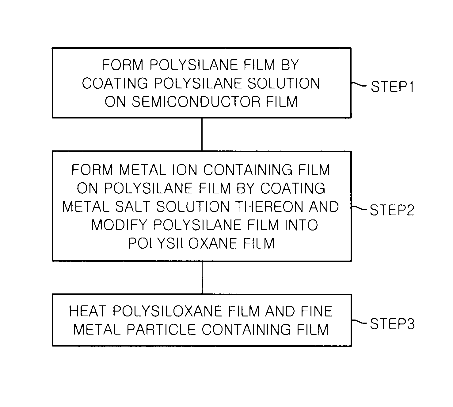
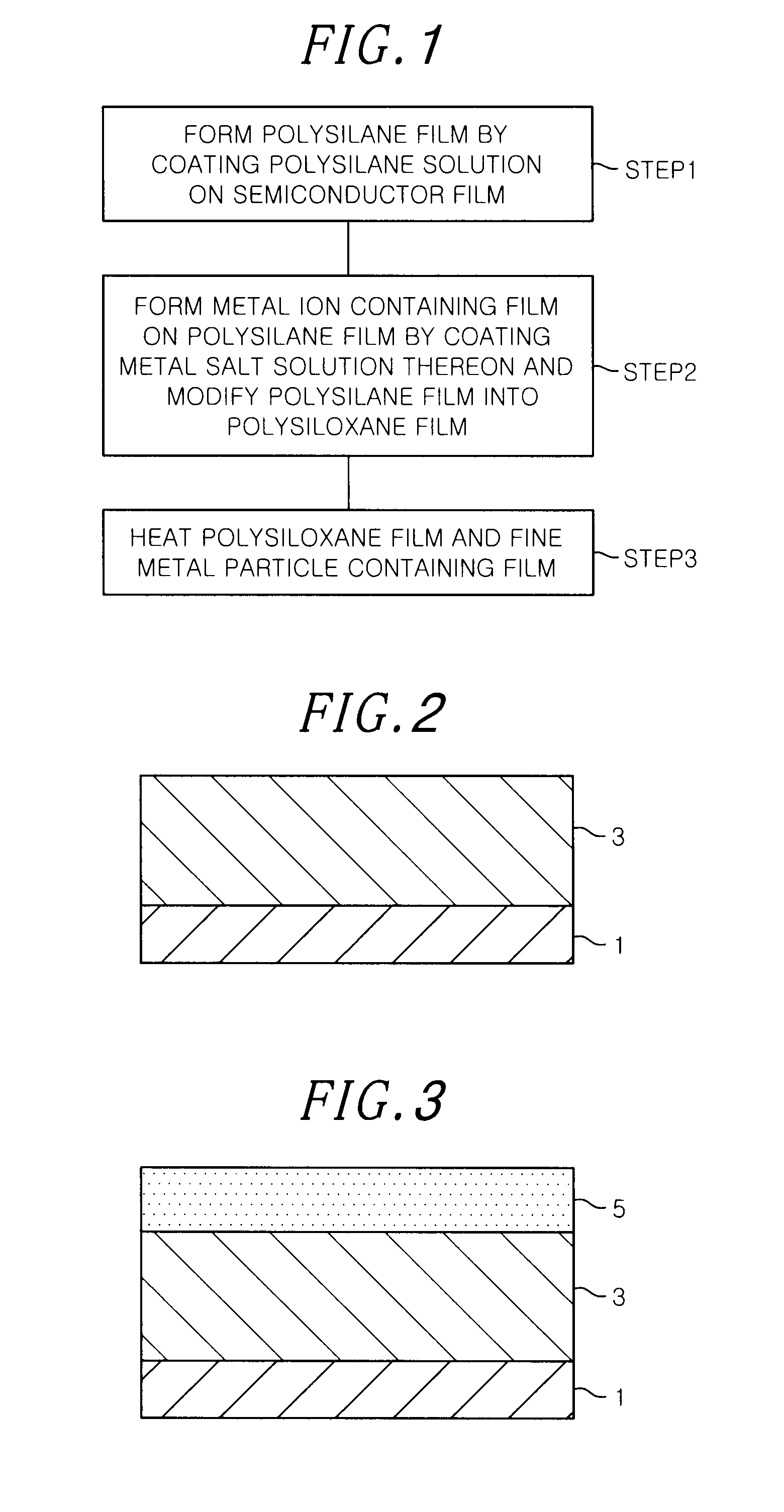
[0033](First Embodiment)

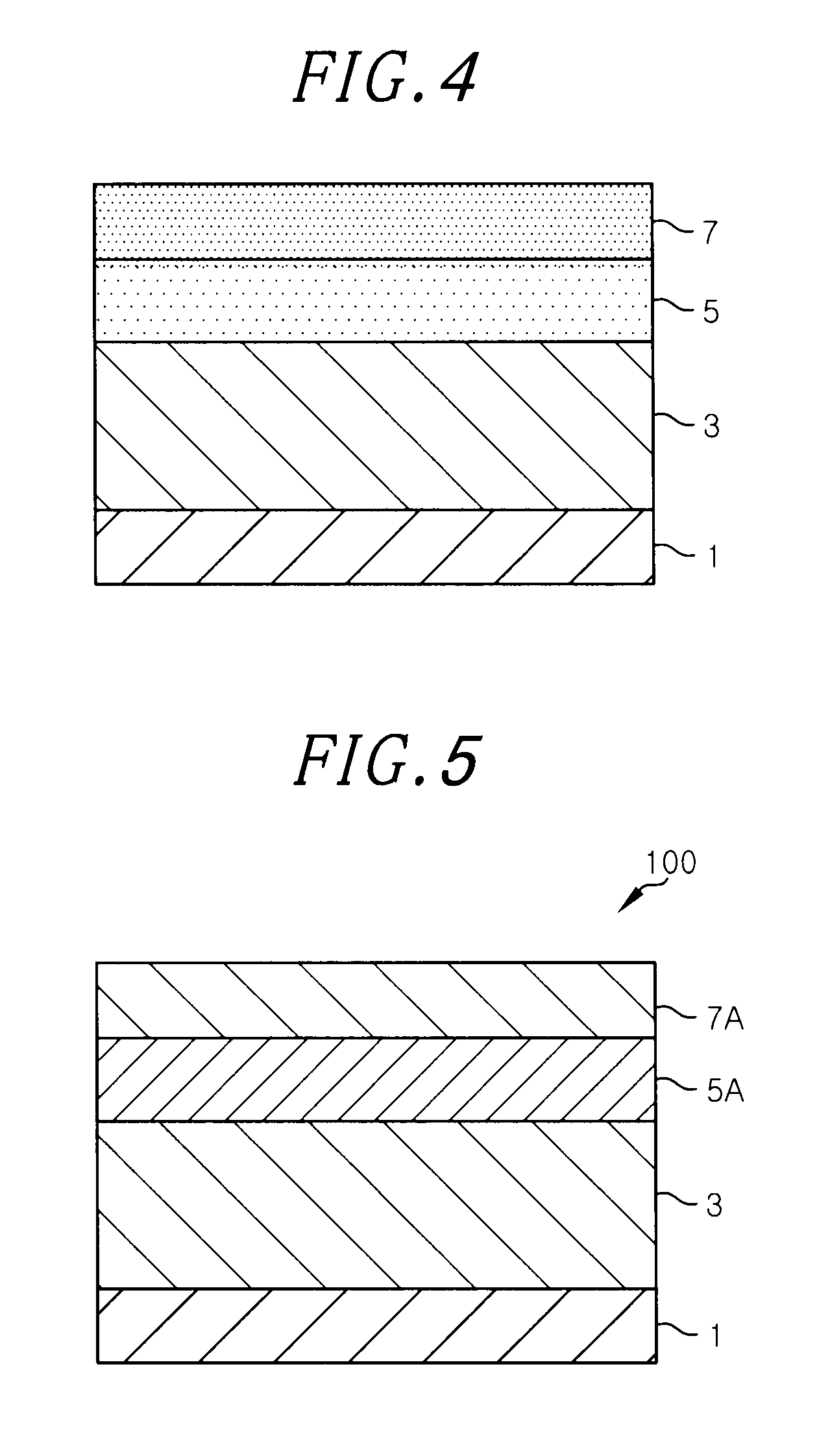
[0034]A film forming method in accordance with a first embodiment of the present invention will be described hereinafter with reference to FIGS. 1 to 5. FIG. 1 is a flowchart showing major steps of the film forming method in accordance with the first embodiment. FIGS. 2 to 5 show the steps of the film forming method in accordance with the first embodiment. In the present embodiments, a stacked substrate having a MOS (Metal Oxide Semiconductor) structure is manufactured.

[0035]First, FIG. 2 is a cross sectional view showing a surface of a substrate serving as a target object to be processed. For example, a base film 1 serving as an insulating film is formed on the surface of the substrate, and a semiconductor film 3 serving as a semiconductor material layer is stacked on the base film 1. In the present embodiment, a silicon film, a silicon carbide film, a gallium nitride film, a zinc oxide film or an organic semiconductor film may be employed as the semiconduct...

second embodiment

[0060](Second Embodiment)

[0061]Next, a film forming method in accordance with a second embodiment of the present invention will be described with reference to FIGS. 6 and 7. FIG. 6 is a flowchart showing major steps of the film forming method of the second embodiment, and FIG. 7 shows the steps of the film forming method of the second embodiment. Similarly, in the present embodiment, a stacked substrate 100A of a MOS structure in use for, e.g., a transistor is manufactured.

[0062](Step 11 and Step 12)

[0063]Step 11 and step 12 are respectively identical to step and step 2 of the first embodiment. Accordingly, the present embodiment will be described by using FIGS. 2 to 5, and thus redundant description thereof will be omitted herein.

[0064](Step 13: Electroless Plating)

[0065]Next, in step 13, a metal film 9 is formed by performing electroless plating by use of a film containing fine metal particles as a plating catalyst (plating core) as shown in FIG. 7.

[0066]A plating bath in use for ...

third embodiment

[0074](Third Embodiment)

[0075]Next, a method of manufacturing a semiconductor device in accordance with the third embodiment of the present invention will be described with reference to FIGS. 8 to 13. FIG. 8 is a flowchart showing major steps of the semiconductor device manufacturing method of the third embodiment. FIGS. 9 to 13 show the steps of the semiconductor device manufacturing method of the third embodiment. Similarly, in the present embodiment, a stacked substrate 101 of a MOS structure in use for, e.g., a transistor is manufactured.

[0076](Step 21: Forming Polysilane Film)

[0077]Step 21 of the present embodiment is identical to step 1 of the first embodiment. Accordingly, the present embodiment will be described by using FIGS. 2 and 3 of the first embodiment, and thus redundant description thereof will be omitted herein.

[0078](Step 22)

[0079]Next, in step 22, from the state shown in FIG. 3, a monomolecular film 11 is formed on the polysilane film 5 as shown in FIG. 9. The mon...


PUM

PropertyMeasurementUnit
thicknessaaaaaaaaaa
thicknessaaaaaaaaaa
thicknessaaaaaaaaaa

Abstract

In a method for forming a stacked substrate of a MOS (Metal Oxide Semiconductor) structure including an oxide film serving as a gate insulating film formed on a semiconductor material layer having a film or substrate shape; and a conductive film serving as a gate electrode formed on the oxide film, a polysilane film on the semiconductor material layer is formed by coating a polysilane solution on a surface of a substrate to which the semiconductor material layer is exposed. A film containing metal ions is formed on the polysilane film by coating a metal salt solution thereon, and the polysilane film and the film containing metal ions are respectively modified into a polysiloxane film and a film containing fine metal particles to form the stacked substrate.

Description

CROSS-REFERENCE TO RELATED APPLICATIONS[0001]This application claims priority to Japanese Patent Application No. 2010-203923 filed on Sep. 13, 2010, the entire contents of which are incorporated herein by reference.FIELD OF THE INVENTION[0002]The present invention relates to a film forming method, a method for manufacturing a semiconductor device by using the film forming method, a semiconductor device and a substrate processing apparatus that can be used in the method.BACKGROUND OF THE INVENTION[0003]Typically, in the manufacturing process of a semiconductor device such as a transistor, an insulating film or a metal film is formed on a substrate, e.g., a semiconductor wafer and, then, the formed film is processed into a desired shape by forming a pattern by employing a photolithographic technique and etching. In the manufacturing process, a film forming process using CVD (Chemical Vapor Deposition), a dry etching process, an asking process and the like are repeated. Almost all of t...

Claims


Application Information

Patent Timeline
Patent Type & Authority Patents(United States)
IPC IPC(8): H01L21/283H01L21/30
CPCH01L21/02348H01L21/76802H01L21/76874H01L21/28264H01L21/02211H01L21/32051H01L29/2003H01L21/02271H01L21/445H01L29/1608H01L29/22H01L21/0223H01L21/28026H01L29/51H01L29/4908H01L21/28158H01L21/67069H01L51/0055H01L51/0537H01L51/0094H01L29/49H10K85/623H10K10/478H10K85/40
Inventor MIYOSHI, HIDENORIAZUMO, SHUJI
Owner TOKYO ELECTRON LTD
Why Eureka
Try Eureka