Oxide semiconductor memory device

a memory device and semiconductor technology, applied in semiconductor devices, digital storage, instruments, etc., can solve the problems of multi-level memory devices, increase in size and cost, etc., and achieve the effects of adequate power consumption reduction, simplified circuit configuration, and extremely long storage tim

Active Publication Date: 2014-07-29
SEMICON ENERGY LAB CO LTD
View PDF147 Cites 12 Cited by
  • Summary
  • Abstract
  • Description
  • Claims
  • Application Information

AI Technical Summary

Benefits of technology

[0014]Multilevel memory devices use many different voltage values accompanying the increase in storage capacity and thus the number of circuits needed is increased, which leads to growth in size and cost increase. This is a problem for multilevel memory devices.
[0015]In view of the problem, an object of one embodiment of the invention disclosed herein is to provide a semiconductor device with a novel structure in which stored data can be retained even when power is not supplied, and does not have a limitation on the number of writing. Further, another object is to simplify the semiconductor device by employing the novel structure and further to increase the storage capacity per unit area.

Problems solved by technology

Multilevel memory devices use many different voltage values accompanying the increase in storage capacity and thus the number of circuits needed is increased, which leads to growth in size and cost increase.
This is a problem for multilevel memory devices.

Method used


Image

  • Oxide semiconductor memory device
  • Oxide semiconductor memory device
  • Oxide semiconductor memory device

Examples


embodiment 1

(Embodiment 1)

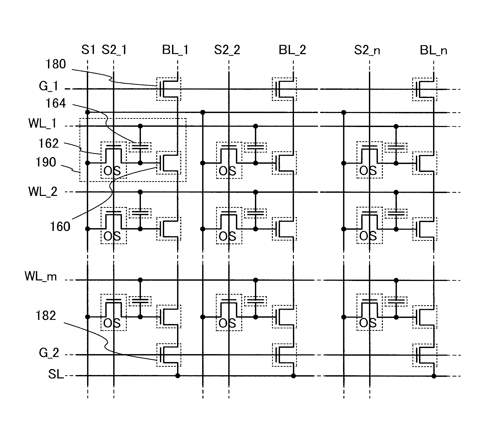
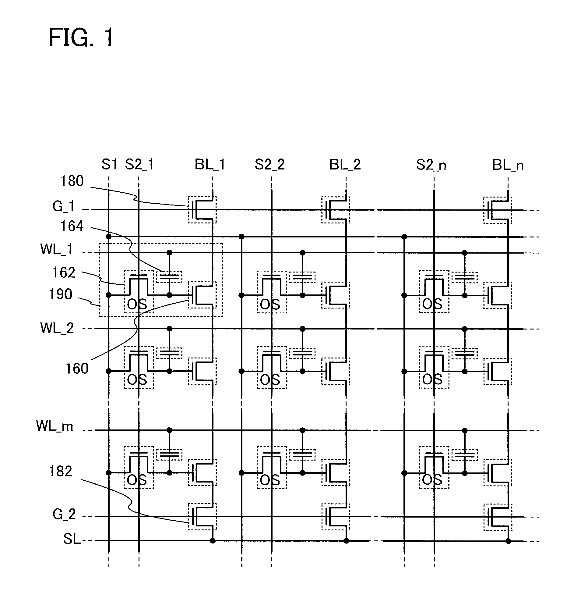
[0068]In this embodiment, a circuit configuration and an operation of a semiconductor device according to one embodiment of the disclosed invention will be described with reference to FIG. 1, FIGS. 2A-1, 2A-2, and 2B, FIG. 3, FIG. 4, FIG. 5, FIG. 6, FIG. 7, and FIG. 8. Note that in each of circuit diagrams, in some cases, “OS” is written beside a transistor in order to indicate that the transistor includes an oxide semiconductor.

[0069]In the semiconductor device in this embodiment, a signal line for controlling on / off of a writing transistor for conducting a writing operation on a memory cell is disposed along a bit line. Further, in the driving method of the semiconductor device, a multilevel writing operation is conducted with use of, also in a writing operation, a voltage which is applied to a capacitor at a reading operation.

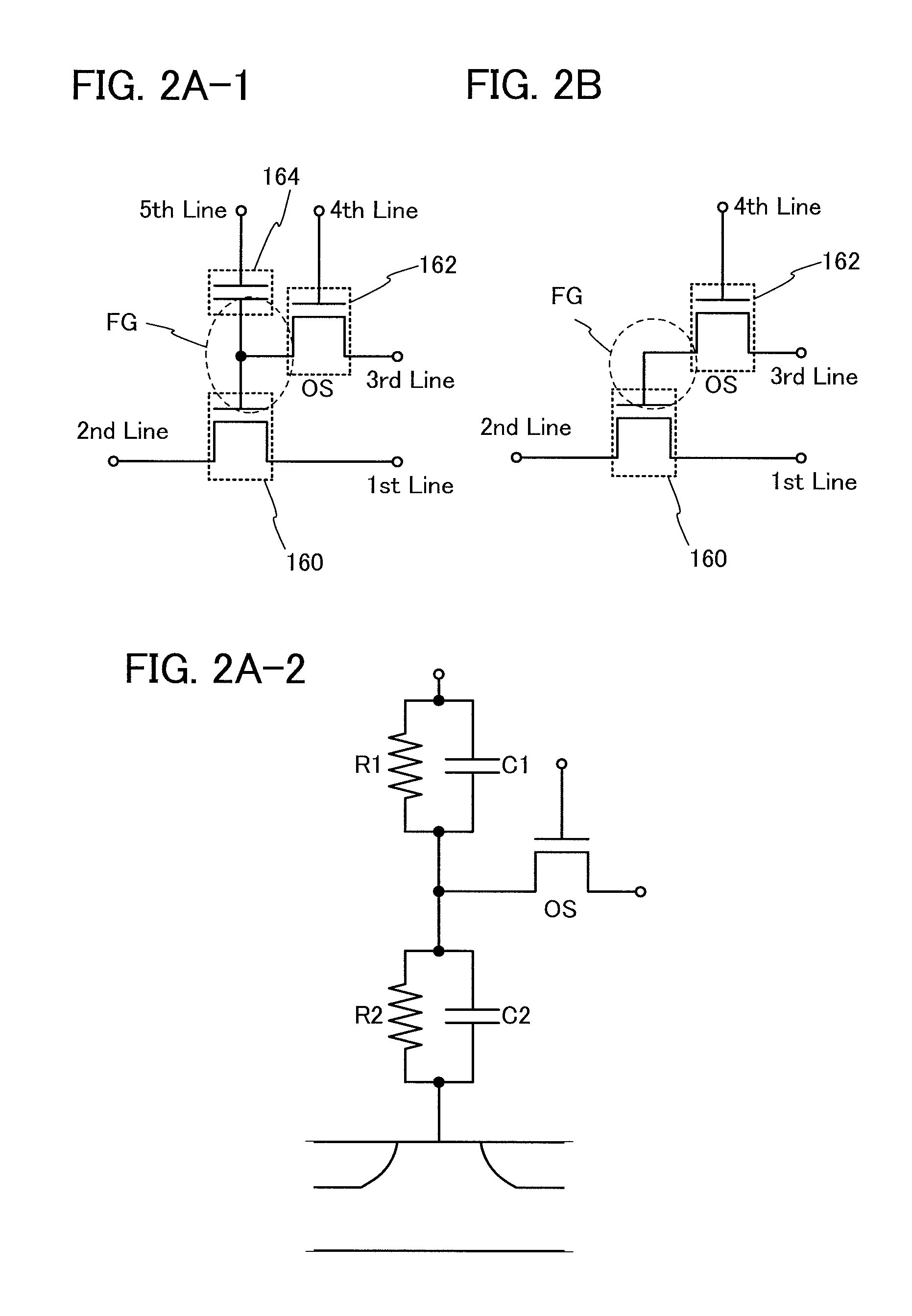
[0070]First, a basic circuit configuration and its operation will be described with reference to FIGS. 2A-1, 2A-2, and 2B. In a semiconductor ...

embodiment 2

(Embodiment 2)

[0130]In this embodiment, a structure and a manufacturing method of a semiconductor device according to one embodiment of the disclosed invention will be described with reference to FIG. 5 and FIGS. 9A and 9B, FIGS. 10A to 10D, FIGS. 11A to 11D, FIGS. 12A to 12D, and FIGS. 13A to 13C.

[0131]FIGS. 9A and 9B show an example of a structure of the memory cell 190 of the semiconductor device illustrated in the circuit diagram of FIG. 5. FIG. 9A illustrates a cross section of the semiconductor device, and FIG. 9B illustrates a plan view of the semiconductor device. Note that, in the plan view illustrated in FIG. 9B, the drawing is simplified without the insulating layer 154, the insulating layer 172, the wiring 171 and the wiring 158 illustrated. Here, in FIG. 9A, the direction parallel to the line A1-A2 of FIG. 9B corresponds to the column direction in the circuit diagram of FIG. 5, and the direction perpendicular to the line A1-A2 of FIG. 9B corresponds to the row direction...

embodiment 3

(Embodiment 3)

[0270]In this embodiment, an example of a transistor that can be applied to a semiconductor device disclosed in this specification will be described. There is no particular limitation on the structure of the transistor that can be applied to a semiconductor device disclosed in this specification; for example, a staggered type or a planar type having a top-gate structure or a bottom-gate structure can be employed. The transistor may have a single-gate structure in which one channel formation region is formed, a double-gate structure in which two channel formation regions are formed, or a triple-gate structure in which three channel formation regions are formed. Alternatively, the transistor may have a dual gate structure including two gate electrode layers positioned over and below a channel formation region with a gate insulating layer provided therebetween.

[0271]FIGS. 15A to 15D each illustrate an example of a cross-sectional structure of a transistor that can be appl...


PUM


Abstract

In a semiconductor device which conducts multilevel writing operation and a driving method thereof, a signal line for controlling on / off of a writing transistor for conducting a writing operation on a memory cell using a transistor including an oxide semiconductor layer is disposed along a bit line, and a multilevel writing operation is conducted with use of, also in a writing operation, a voltage which is applied to a capacitor at a reading operation. Because an oxide semiconductor material that is a wide gap semiconductor capable of sufficiently reducing off-state current of a transistor is used, data can be held for a long period.

Description

BACKGROUND OF THE INVENTION[0001]1. Field of the Invention[0002]One embodiment of the disclosed invention relates to a semiconductor device using a semiconductor element and a method for driving the semiconductor device.[0003]2. Description of the Related Art[0004]Storage devices using semiconductor elements are broadly classified into two categories: a volatile device that loses stored data when power supply stops, and a non-volatile device that retains stored data even when power is not supplied.[0005]A typical example of a volatile storage device is a DRAM (dynamic random access memory). A DRAM stores data in such a manner that a transistor included in a memory element is selected and electric charge is stored in a capacitor.[0006]When data is read from a DRAM, electric charge in a capacitor is lost on the above-described principle; thus, another writing operation is necessary whenever data is read out. Moreover, since leakage current (off-state current) or the like flows between...

Claims


Application Information

Patent Timeline
Patent Type & Authority Patents(United States)
IPC IPC(8): G11C11/34G11C11/24
CPCH01L27/1225G11C11/403H01L27/11517H01L27/1156G11C16/0433G11C16/0483H10B41/00H10B41/70H10B99/00H10B12/00
Inventor OHNUKI, TATSUYA
Owner SEMICON ENERGY LAB CO LTD
Why Eureka
Try Eureka