Method of optimizing a GA—nitride device material structure for a frequency multiplication device

a frequency multiplication and nitride technology, applied in the direction of cad circuit design, computer aided design, semiconductor devices, etc., can solve the problems of affecting reliability and power transfer, increasing power absorbed in the varactor, and little in the conceptual field of conceptual methods, and achieves good crystalline and greater conversion efficiency

Inactive Publication Date: 2014-08-05
US SEC THE ARMY THE
View PDF3 Cites 5 Cited by
  • Summary
  • Abstract
  • Description
  • Claims
  • Application Information

AI Technical Summary

Benefits of technology

[0005]A preferred embodiment of the present invention comprises a semi-insulator GaN (or SiC, or AN) substrate anti-serial Schottky varactor for efficient power-selective microwave to sub-millimeter wave frequency signal multiplier involving varying the aluminum composition of an AlGaN barrier layer to maximize, inter alia, output power efficiency. In place of the AlGaN barrier, any semi-insulating layer with energy gap greater than 3.5 and free carrier mobility less than 300 cm2 / V / s may be used. This list would include properly grown and doped diamond or boron-nitride appropriately grown for good crystalline quality on GaN. In a preferred methodology, selection of AlGaN / GaN varactors containing either (1) a high-doped / low-doped GaN region or (2) just a low doped GaN region is utilized depending upon the amplitude of the input signal being tripled in frequency. Stronger susceptance modulation is exhibited in AlGaN / GaN Anti-series Schottky Varactors (ASVs) made from Ga-face polar material compared to N-face polar material. Results indicate that as a frequency tripler choosing the proper aluminum composition results in 27% conversion efficiency with an input signal of 5 GHz and over 7% conversion efficiency with an input signal of 60 GHz along with optimization trends. With input voltage amplitudes over 10 V, an AlGaN / GaN structure with 15% Al provides greater conversion efficiency than one with 5% Al. Power absorbed in the varactor also increases as aluminum percent increases, affecting reliability and power transfer. Results of a GaN-based ASV performing as a frequency tripler for fundamental frequencies up to 110 GHz indicate an advantage to using an AlGaN / GaN epi-structure over only a GaN epi-structure.

Problems solved by technology

However, little has been done insofar as a conceptual method on how to optimize the device-material structure for highest frequency conversion efficiency at a particular output power level.
Power absorbed in the varactor also increases as aluminum percent increases, affecting reliability and power transfer.

Method used


Image

  • Method of optimizing a GA—nitride device material structure for a frequency multiplication device
  • Method of optimizing a GA—nitride device material structure for a frequency multiplication device
  • Method of optimizing a GA—nitride device material structure for a frequency multiplication device

Examples


Embodiment Construction

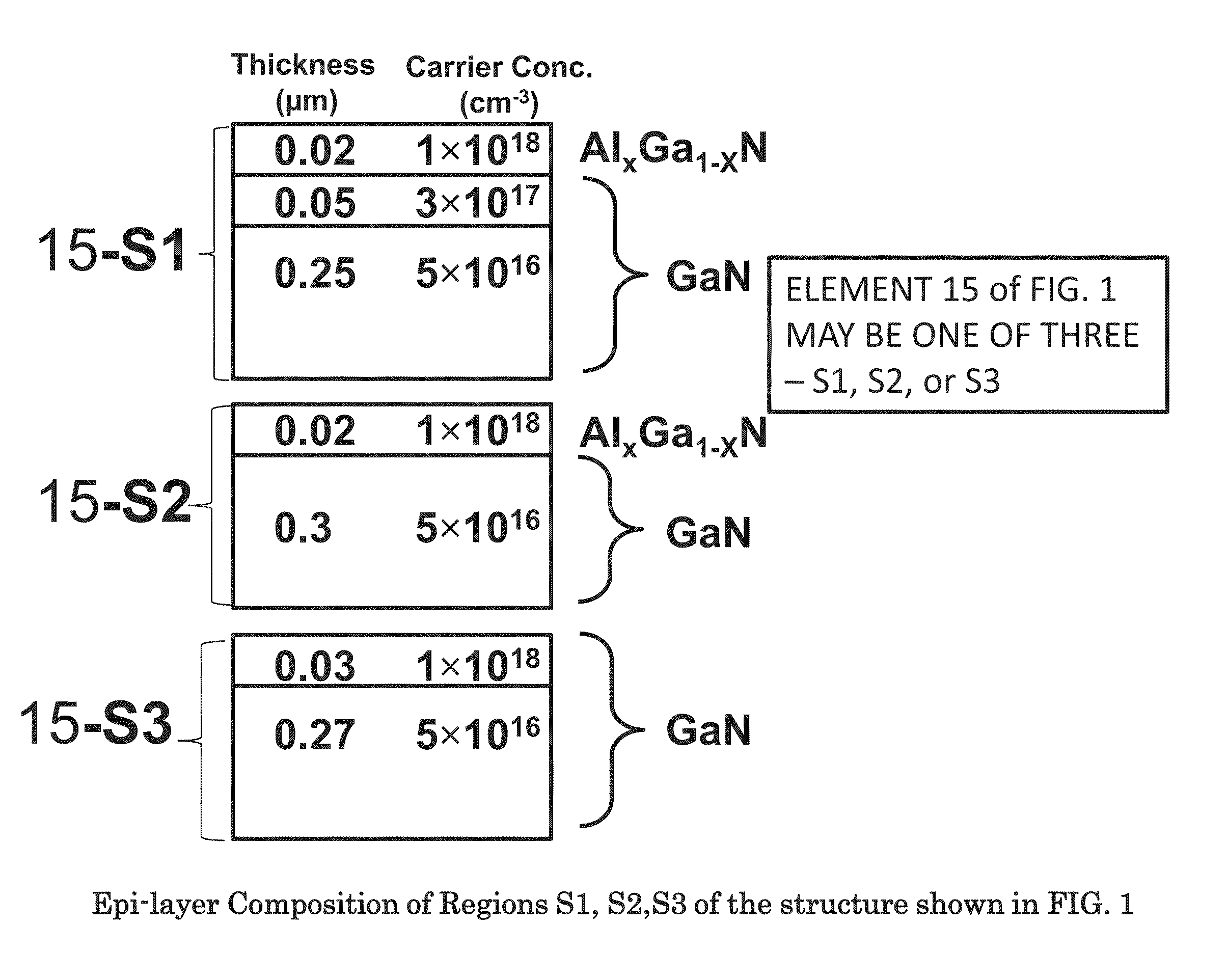
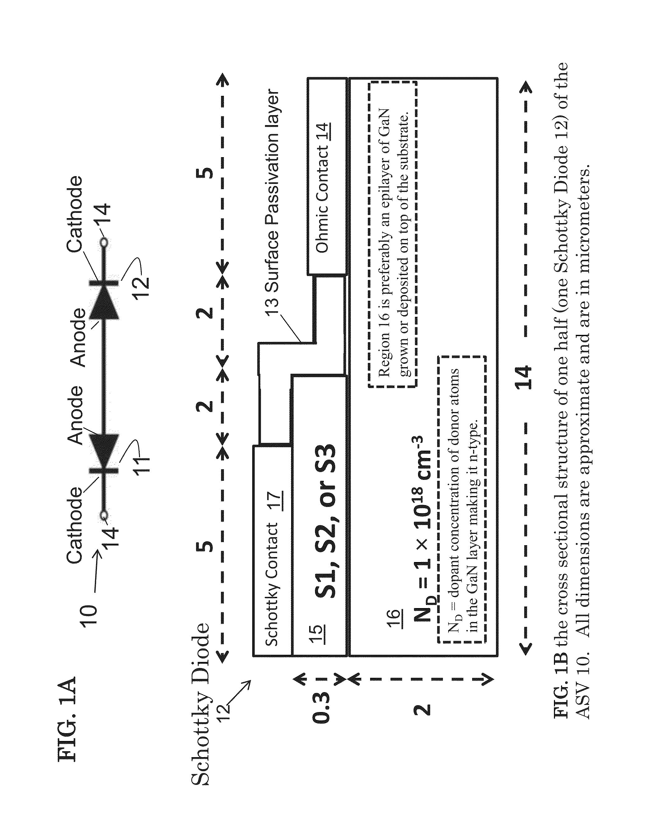
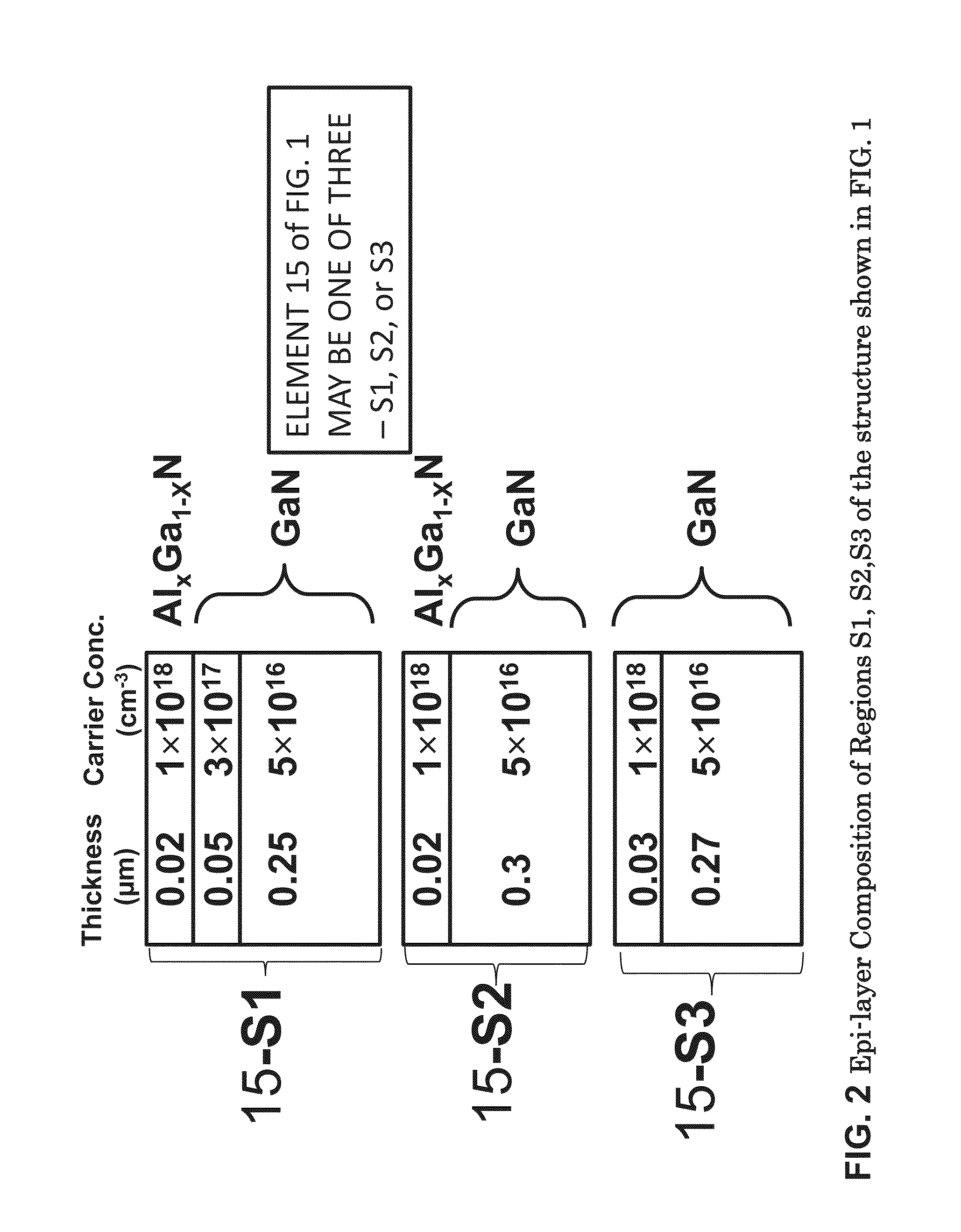
[0051]The embodiments of the invention and the various features and advantageous details thereof are explained more fully with reference to the non-limiting embodiments that are illustrated in the accompanying drawings and detailed in the following description. It should be noted that the features illustrated in the drawings are not drawn to scale. Descriptions of well-known components and processing techniques are omitted so as to not unnecessarily obscure the embodiments of the invention. The examples used herein are intended merely to facilitate an understanding of ways in which the embodiments of the invention may be practiced and to further enable those of skill in the art to practice the embodiments of the invention. Accordingly, the examples should not be construed as limiting the scope of the embodiments of the invention. Rather, these embodiments are provided so that this disclosure will be thorough and complete, and will fully convey the scope of the invention to those ski...


PUM


Abstract

A preferred method of optimizing a Ga-nitride device material structure for a frequency multiplication device comprises:
    • determining the amplitude and frequency of the input signal being multiplied in frequency;
    • providing a Ga-nitride region on a substrate;
    • determining the Al percentage composition and impurity doping in an AlGaN region positioned on the Ga-nitride region based upon the power level and waveform of the input signal and the desired frequency range in order to optimize power input/output efficiency; and
    • selecting an orientation of N-face polar GaN or Ga-face polar GaN material relative to the AlGaN/GaN interface so as to orient the face of the GaN so as to optimize charge at the AlGaN/GaN interface. A preferred embodiment comprises an anti-serial Schottky varactor comprising: two Schottky diodes in anti-serial connection; each comprising at least one GaN layer designed based upon doping and thickness to improve the conversion efficiency.

Description

GOVERNMENT INTEREST[0001]The embodiments herein may be manufactured, used, and / or licensed by or for the United States Government without the payment of royalties thereon.BACKGROUND OF THE INVENTION[0002]A frequency multiplier (e.g. a tripler) is a device that, as an example, takes an input signal at 30 GHz and converts some of the energy from this input signal into an output signal at 90 GHz. Because a frequency multiplier is used to generate an output at a different frequency from the input, one of the goals of an optimized structure is efficient operation whereby the energy transferred to the new frequency at the output is maximized. The same methodology for the device / structure and optimization can also be applied to obtain higher harmonics, such as the fifth order of conversion, which will be useful for sub-millimeter wave signal generation.[0003]Varactor multipliers have first been conceptualized back in the mid 1960s. However, little has been done insofar as a conceptual meth...

Claims


Application Information

Patent Timeline
Patent Type & Authority Patents(United States)
IPC IPC(8): H01L21/338
CPCH01L29/2003H01L29/205H01L29/93G06F17/5068H01L29/872H01L29/22H01L29/1608H01L29/66174
Inventor SHAH, PANKAJ B.HUNG, H. ALFRED
Owner US SEC THE ARMY THE
Why Eureka
Try Eureka