Analog transcap device

a transcap and analog technology, applied in the field of semiconductor devices, can solve the problems of distorted capacitance value, inability to obtain an extremely high capacitance value, and inability to add unacceptable levels of inter-modulation, so as to avoid distortion and increase the performance of the device

Active Publication Date: 2014-08-12
QUALCOMM INC
View PDF6 Cites 35 Cited by
  • Summary
  • Abstract
  • Description
  • Claims
  • Application Information

AI Technical Summary

Benefits of technology

[0019]The present invention describes a MOS based semiconductor variable capacitor structure, named transcap, suitable for integrated circuits, which has at least three terminals, one of which is used to modulate the equivalent capacitor area of the MOS structure by increasing or decreasing its DC voltage with respect to another terminal of the device, in order to change the capacitance over a wide range of values. Furthermore, the present invention decouples the AC signal and the DC control voltage avoiding distortions and increasing the performance of the device, such as control reliability. The present invention is simple and only slightly dependent on the variations related to the fabrication process.

Problems solved by technology

Their use is limited to low signal amplitudes to avoid obvious distortions as the capacitance would be affected by the change of signal voltage, precluding their use in the input stages of high-quality RF communications receivers, where they would add unacceptable levels of inter-modulation.
Furthermore an extremely high value of capacitance cannot be obtained even with a reverse bias because the reverse-biased saturation current is not exactly equal to zero.
This leads to the disadvantage that the AC voltage is superimposed upon the DC control value, and therefore the capacitance value is distorted by the AC voltage.
As underlined by the author himself in the patent, they are not suitable for integrated circuits.
In this case, as in the previous one, both the depletion regions in the p and n regions are used to modulate the capacitance, which lead to a difficult control of the device performance and capacitance-voltage relation (the process variations of the p-region sum up with the one of the N region and to the variability on the position of the pn-junction).
Furthermore, in all these structures, the DC voltage is applied between one terminal of the capacitance and a region directly in contact with the capacitance dielectric layer overlapping the metal terminal 27 in FIG. 1 (or 45 in FIG. 3), causing a distortion of the capacitance value due to the modulation of the MOS capacitance.
Furthermore, in this configuration the capacitance depends also on the thickness of the depletion regions of the two p+ / n junction as in conventional diode based varactors, leading to a high distortion of the capacitance value.

Method used


Image

  • Analog transcap device
  • Analog transcap device
  • Analog transcap device

Examples


Embodiment Construction
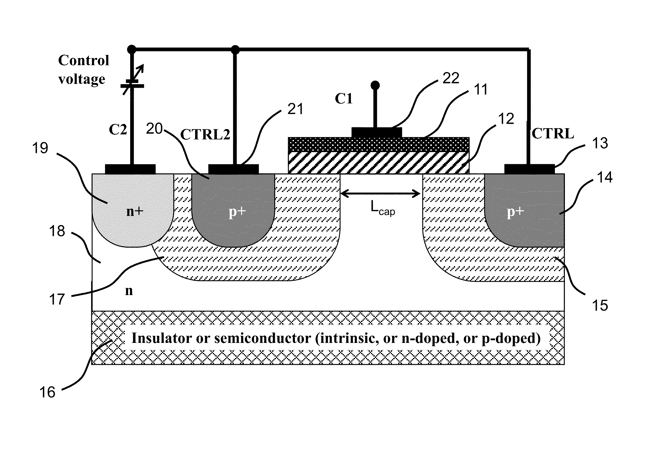
A FIG. 1

[0137]FIG. 1 is showing the preferred embodiment of the invention as described in the regular patent application U.S. Ser. No. 13 / 068,161 entitled “Semiconductor Variable Capacitor”, filed by the same applicants on May 5, 2011. The pt type region 5 defines the control terminal of the device whereas the region 2 and the n+ region 8 are the two terminals of the capacitor. Region 3 corresponds to the capacitor dielectric layer, whereas region 10 is a n-type semiconductor layer. xL is the distance between the capacitance plate 2 and the p+ control region 5, whereas L is the length of the lower effective capacitance plate 2. The lower capacitance plate is constituted by the neutral region of the semiconductor layer 10, and is connected to the C2 terminal 9 through the n+ region 8. The C1 electrode 2 may be built in poly-silicon or metal.
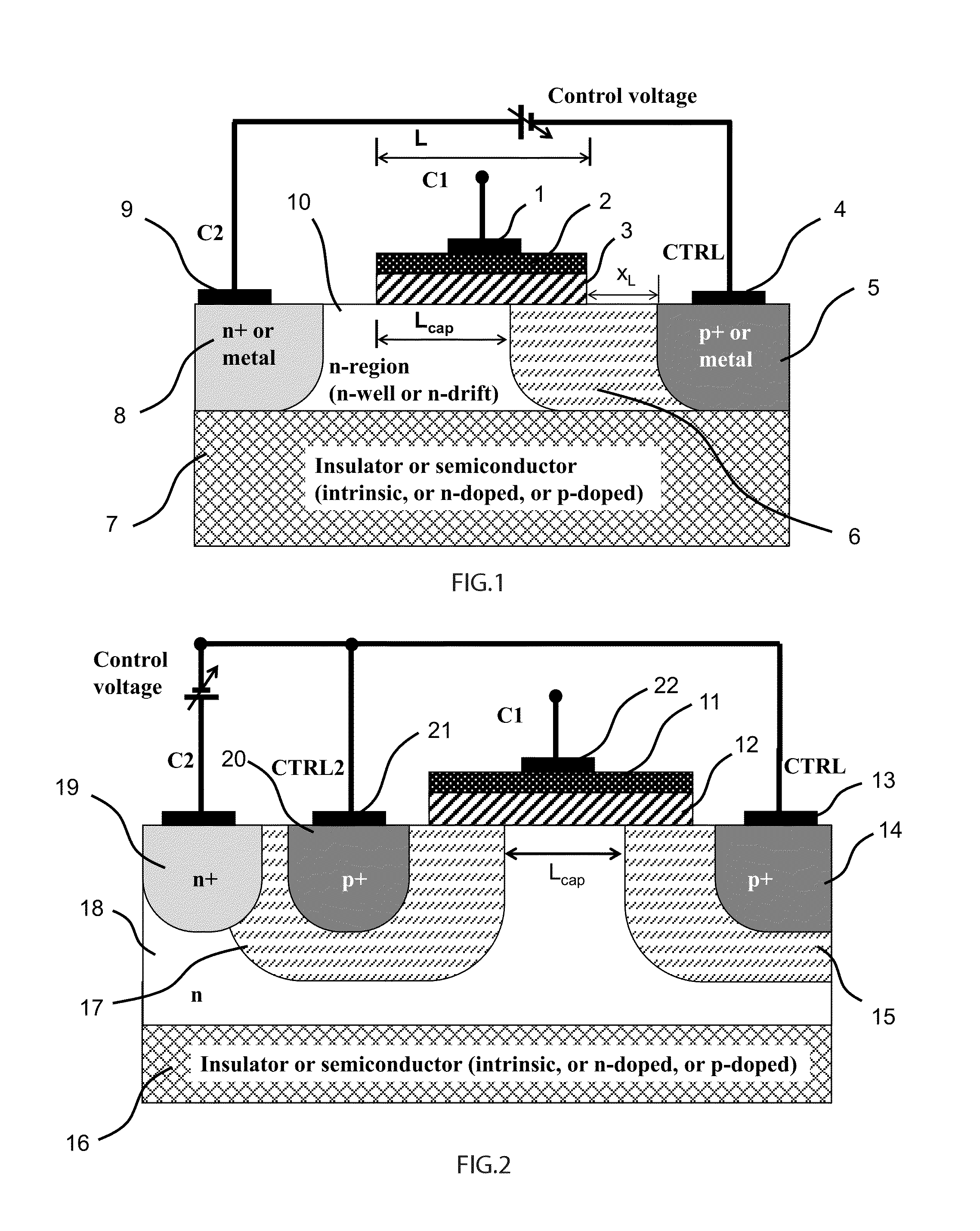
B FIG. 2

[0138]FIG. 2 is depicting the cross-section view of a semiconductor variable capacitor according to a further embodiment of the invention...


PUM


Abstract

A novel semiconductor variable capacitor is presented. The semiconductor structure is simple and is based on a semiconductor variable MOS capacitor structure suitable for integrated circuits, which has at least three terminals, one of which is used to modulate the equivalent capacitor area of the MOS structure by increasing or decreasing its DC voltage with respect to another terminal of the device, in order to change the capacitance over a wide ranges of values. Furthermore, the present invention decouples the AC signal and the DC control voltage avoiding distortion and increasing the performance of the device, such as its control characteristic. The present invention is simple and only slightly dependent on the variations due to the fabrication process. It exhibits a high value of capacitance density and, if opportunely implemented, shows a quasi linear dependence of the capacitance value with respect to the voltage of its control terminal.

Description

RELATED APPLICATION DATA[0001]The present application is a continuation in part of the regular patent application U.S. Ser. No. 13 / 068,161 entitled “Semiconductor Variable Capacitor”, filed on May 5, 2011. Furthermore, the present patent application claims priority also from the following U.S. Provisional Patent Application 61 / 644,070 for “Semiconductor controllable capacitor” filed on May 8, 2012, U.S. 61 / 709,907 for “Transcap Semiconductor variable capacitor” filed on Oct. 4, 2012, U.S. 61 / 772,461 for “Variable Capacitor Circuit Applications” filed on Mar. 4, 2013.BACKGROUND OF THE INVENTION[0002]1. Field of the Invention[0003]The present invention is in the field of semiconductor structures. The present invention is further in the field of semiconductor structures of variable capacitance devices. Particularly, it relates to a MOS type variable capacitance device for semiconductor circuits. The implementation is not limited to a specific technology, and applies to either the inven...

Claims


Application Information

Patent Timeline
Patent Type & Authority Patents(United States)
IPC IPC(8): H01L29/93H01L27/12
CPCH01L29/93H01G7/06H01G7/00H01L29/94
Inventor MARINO, FABIO ALESSIOMENEGOLI, PAOLO
Owner QUALCOMM INC
Why Eureka
Try Eureka