Compliant wafer level probe assembly

a wafer-level, probe-type technology, applied in the direction of electronic circuit testing, measurement devices, instruments, etc., can solve the problems of reducing the electrical performance of the connection, affecting the self-heating effect of the contact, and the probe is usually more expensive, so as to achieve the effect of improving the electrical performan

Active Publication Date: 2014-08-12
HSIO TECH
View PDF328 Cites 50 Cited by
  • Summary
  • Abstract
  • Description
  • Claims
  • Application Information

AI Technical Summary

Benefits of technology

[0015]The present probe assembly can provide a low cost alternative to other probe products, by utilizing an additive printing process and unique probe member fabrication process. The nature of the process can allow for very high frequency performance, as well as the addition of on-board electrical devices and circuitry planes that are not available with other probe products. The present probe assembly can be superior to membrane probe products in terms of mechanical performance, manufacturing complexity, electrical performance, and cost.
[0016]The production cost for a probe assembly in accordance with the present disclosure can be a fraction of the cost of producing exiting probe cards. The use of additive processes, such as for example, printed electrical features, reduces the capital cost and lead time for building the present probe assemblies. The additive processes can also increase yields over probe systems that rely on conventional lithography tools and masks.
[0017]Internal compliance of the entire assembly and of individual probe members can greatly increase performance of the present probe assemblies. The ability to build multi-layer structures over a relatively large area can permit terminal pitch on the IC devices to be reduced. The addition of circuitry planes and electrical devices in the present probe assembly can provide performance enhancements not available with current probe systems. The ability to add electrical devices, such as transistors and memory, to the present probe assembly can provide the opportunity to incorporate test intelligence, extending the use of legacy test equipment and improving test performance. The present probe assemblies can provide the opportunity to develop adaptive testing and to alter the circuit members during testing.
[0028]The use of additive printing processes can permit the material set in a given layer of a probe assembly to vary. Traditional PCB and circuit fabrication methods take sheets of material and stack them up, laminate, and / or drill. The materials in each layer are limited to the materials in a particular sheet. Additive printing technologies permit a wide variety of materials to be applied on a layer with a registration relative to the features of the previous layer. Selective addition of conductive, non-conductive, or semi-conductive materials at precise locations to create a desired effect has the major advantages in tuning impedance or adding electrical function on a given layer. Tuning performance on a layer by layer basis relative to the previous layer greatly enhances electrical performance.

Problems solved by technology

Long contact members, however, tend to reduce the electrical performance of the connection by creating a parasitic effect that impacts the signal as it travels through the contact.
Resistance in the contacts impacts the self heating effects as current passes through power delivery contacts.
Also, the small space between contacts can cause distortion known as cross talk as a nearby contact may influence its neighbor.
In most cases, the tests that are run using needle probes are typically basic on-off tests due to the limited signal integrity.
These probes are usually more expensive, and are typically used for area array connections.
Again, the length of the contact wire to allow the beam to buckle is relatively large, so the signal performance can be impacted.
Micro spring and MEMS-based probes are typically very expensive, and although better electrically than the longer probe styles, they may have electrical limitations.
Membrane probes typically have the best signal performance, but can be expensive to build.
The manufacturing process is very complicated, with many thin film, plating and lithography steps.
The complexity of the process results in yield loss and the capital requirements are fairly large.
There is a potential for the membrane probe to collect debris and crush it into the wafer, thereby damaging ICS.
Also, the contact tips must be extremely planar relative to the wafer since the probe tips typically have little or no compliance to compensate for non-planarity.
All of these probe types are rather expensive, costing thousands or even hundreds of thousands of dollars, depending on the type and number of contact points required.
Wafer manufactures typically test each device at least once, so durability of the probe tips can be critical.
Next generation systems will operate above 5 GHz and beyond and existing probe cards will not achieve acceptable price / performance levels without significant revision.

Method used


Image

  • Compliant wafer level probe assembly
  • Compliant wafer level probe assembly
  • Compliant wafer level probe assembly

Examples


Embodiment Construction

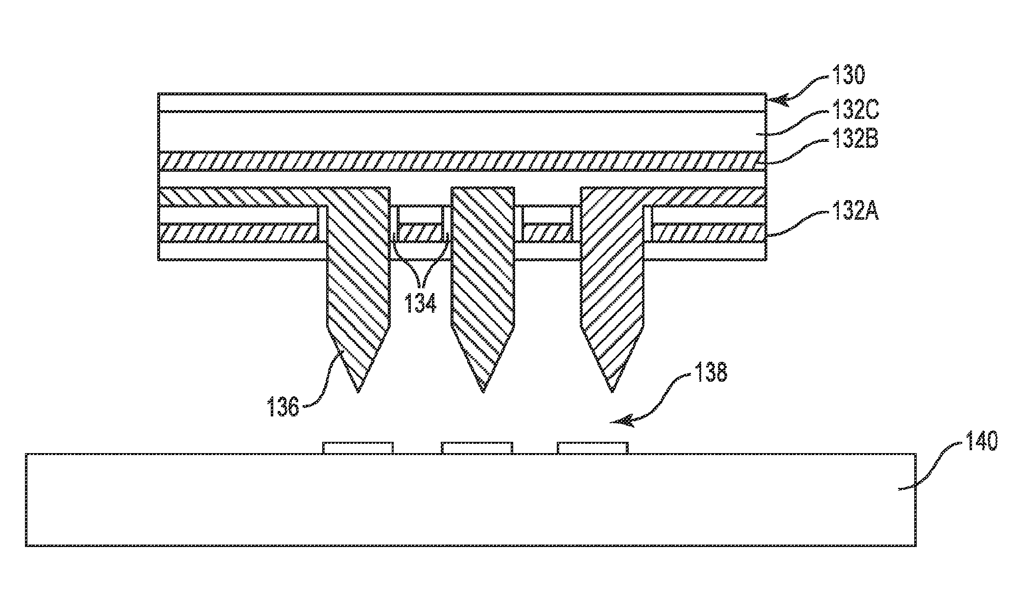
[0043]The present disclosure relates to a high performance probe assembly for testing wafer-level integrated circuits. The present probe assembly can be used with electrical devices having contact-to-contact spacing (pitch) on the order of less than about 1.0 millimeter (1×10⁻³ meters), and more preferably a pitch of less than about 0.7 millimeter, and most preferably a pitch of less than about 0.4 millimeter. Such fine pitch probe assemblies are especially useful for probing wafer-level integrated circuits.

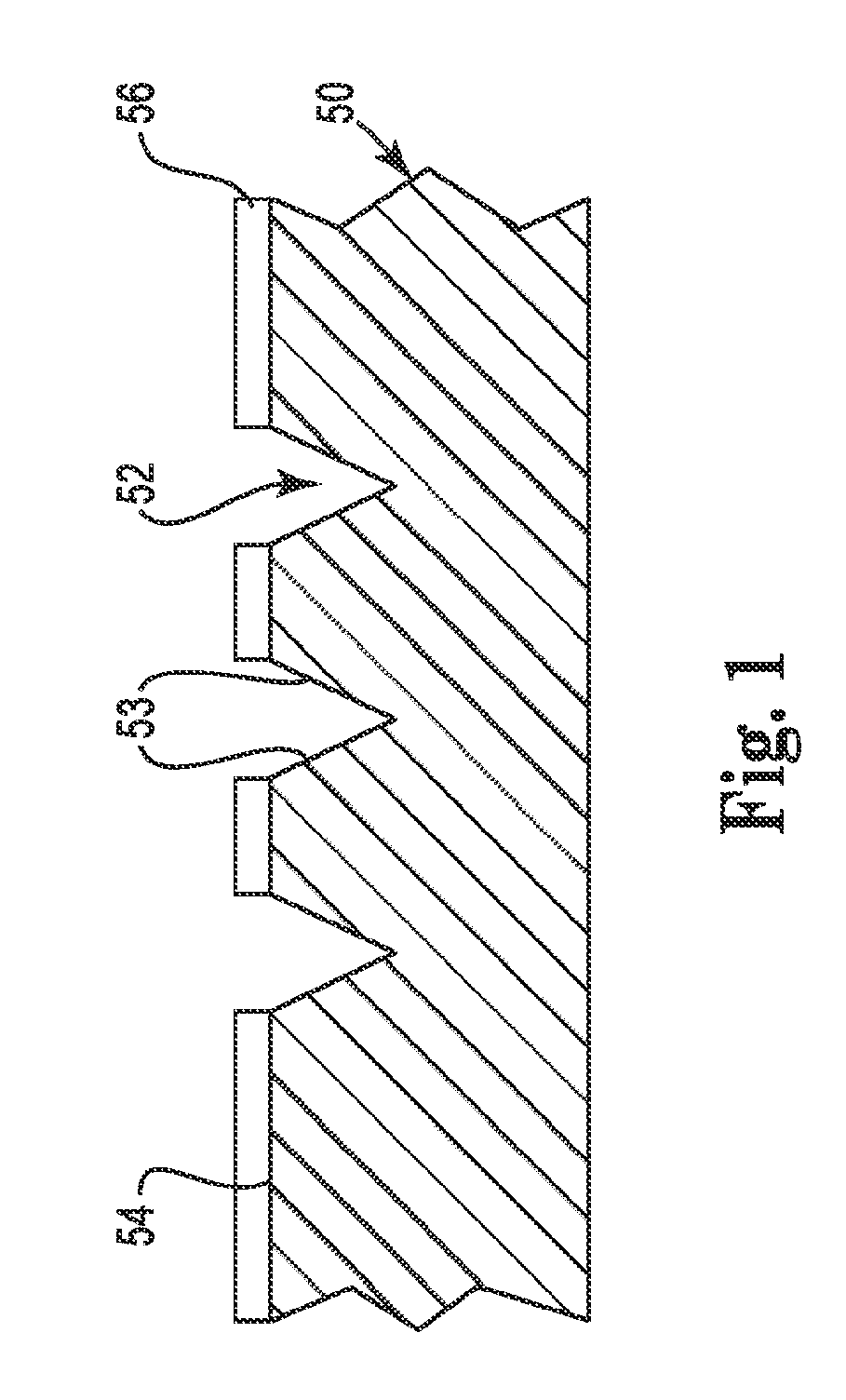
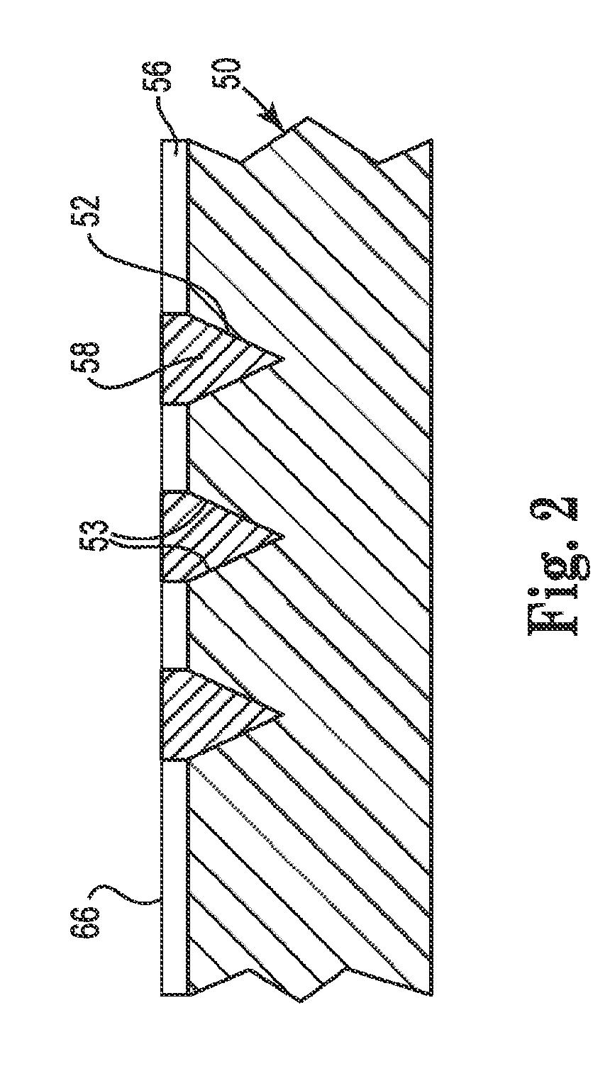
[0044]FIG. 1 is a cross-sectional view of a fixture 50 useful in making a probe assembly, in accordance with an embodiment of the present disclosure. The fixture 50 can include a plurality of cavities 52 in a first surface 54. The locations of the cavities 52 are arranged in an array that corresponds to terminals on a wafer-level IC device (see e.g., FIG. 6). The cavities 52 can be formed using a variety of techniques, such as molding, machining, printing, imprinting, embossing, ...


PUM

PropertyMeasurementUnit
widthaaaaaaaaaa
aspect ratioaaaaaaaaaa
conductiveaaaaaaaaaa

Abstract

A probe assembly that acts as a temporary interconnect between terminals on a circuit member and a test station. The probe assembly can include a base layer of a dielectric material printed onto a surface of a fixture. The surface of the fixture can have a plurality of cavities. A plurality of discrete contact members can be formed in the plurality of cavities in the fixture and coupled to the base layer. A plurality of conductive traces can be printed onto an exposed surface of the base layer and electrically coupled with proximal ends of one or more of the discrete contact members. A compliant layer can be deposited over the conductive traces and the proximal ends of the contact members. A protective layer can be deposited on the compliant layer such that when the probe assembly is removed from the fixture the distal ends of the contact members contact terminals on the circuit member and the conductive traces electrically couple the circuit member to a test station. Electrical devices on the probe assembly can communicate with the test station to provide adaptive testing.

Description

CROSS-REFERENCE TO RELATED APPLICATIONS[0001]This application is a national stage application under 35 U.S.C. §371 of International Application No. PCT / US2010 / 036047, titled COMPLIANT WAFER LEVEL PROBE ASSEMBLY, filed May 25, 2010, which claims priority to United States Provisional Application No. 61 / 183,856, filed Jun. 3, 2009, both of which are hereby incorporated by reference in their entireties.TECHNICAL FIELD[0002]The present disclosure relates to a probe assembly for testing electrical devices, and in particular, to a probe assembly that forms a temporary electrical interconnect between a wafer-level electrical device and a test station.BACKGROUND OF THE INVENTION[0003]During the semiconductor production process, manufacturers typically test integrated circuit (IC) devices while they are still grouped together as built on a silicon wafer. These tests verify various manufacturing parameters as well as chip function when possible. The connection points or terminals that will eve...

Claims


Application Information

Patent Timeline
Patent Type & Authority Patents(United States)
IPC IPC(8): G01R1/067
CPCG01R1/07314Y10T29/49117Y10T29/49004
Inventor RATHBURN, JAMES
Owner HSIO TECH
Why Eureka
Try Eureka