Passivated emitter rear locally patterned epitaxial solar cell

a solar cell and local pattern technology, applied in the field of solar cells, can solve the problems of low manufacturing cost and high cost of cells, and achieve the effects of reducing the free carrier absorption of light, reducing the lifetime of minority carriers, and minimizing the recombination velocity of back surfaces

Active Publication Date: 2014-08-19
SVAGOS TECHNICK INC
View PDF14 Cites 16 Cited by
  • Summary
  • Abstract
  • Description
  • Claims
  • Application Information

AI Technical Summary

Benefits of technology

[0005]Some embodiments of the present invention are PERL-e (Passivated Emitter Rear Local epitaxy) solar cells, which are fabricated with epitaxial deposition processes. The PERL-e solar cells may have some or all of the following advantages. First, a majority of the back side of the PERL-e cell is not heavily doped, unlike either Al fired p+ back surface, boron diffused p+ region or epitaxially grown p+ region solar cells. This significantly reduces free carrier absorption of light in the p+ region as well as reducing minority carrier lifetime in this region due to heavy doping. Second, a high quality lightly doped back surface can be passivated with various dielectric films (such as silicon dioxide, silicon nitride and amorphous silicon) to minimize the back surface recombination velocity. Third, with an epitaxially produced back surface field (BSF) followed by selective etch back of this region, the process of creating heavily boron doped regions can be lower in cost as compared to boron diffusion and better in quality as compared to boron diffused regions or to the use of laser fired contacts. Furthermore, the use of epitaxial back surface fields provides greater freedom in terms of junction depth (p+ layer thickness), junction profiles and dopant concentrations. PERL-e solar cells may be fabricated with either thin or thick silicon.

Problems solved by technology

However, these cells are costly to fabricate since expensive float zone silicon was utilized for the device fabrication and the use of photolithography for metal contact formation is not conducive to low manufacturing cost.
As silicon wafer thickness is reduced to reduce silicon consumption and hence manufacturing costs of photovoltaic products, more of the long wavelength infrared radiation will pass through the thin wafer without being absorbed, due to the relatively poor absorption coefficient of silicon.

Method used


Image

  • Passivated emitter rear locally patterned epitaxial solar cell
  • Passivated emitter rear locally patterned epitaxial solar cell
  • Passivated emitter rear locally patterned epitaxial solar cell

Examples


Embodiment Construction

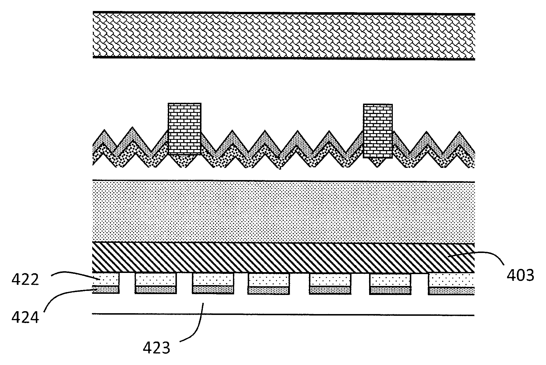
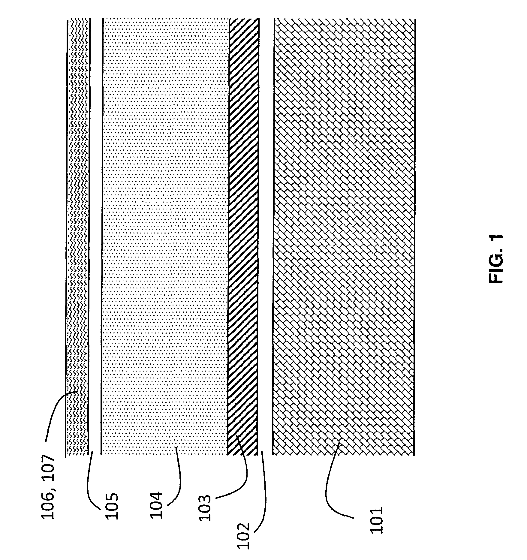
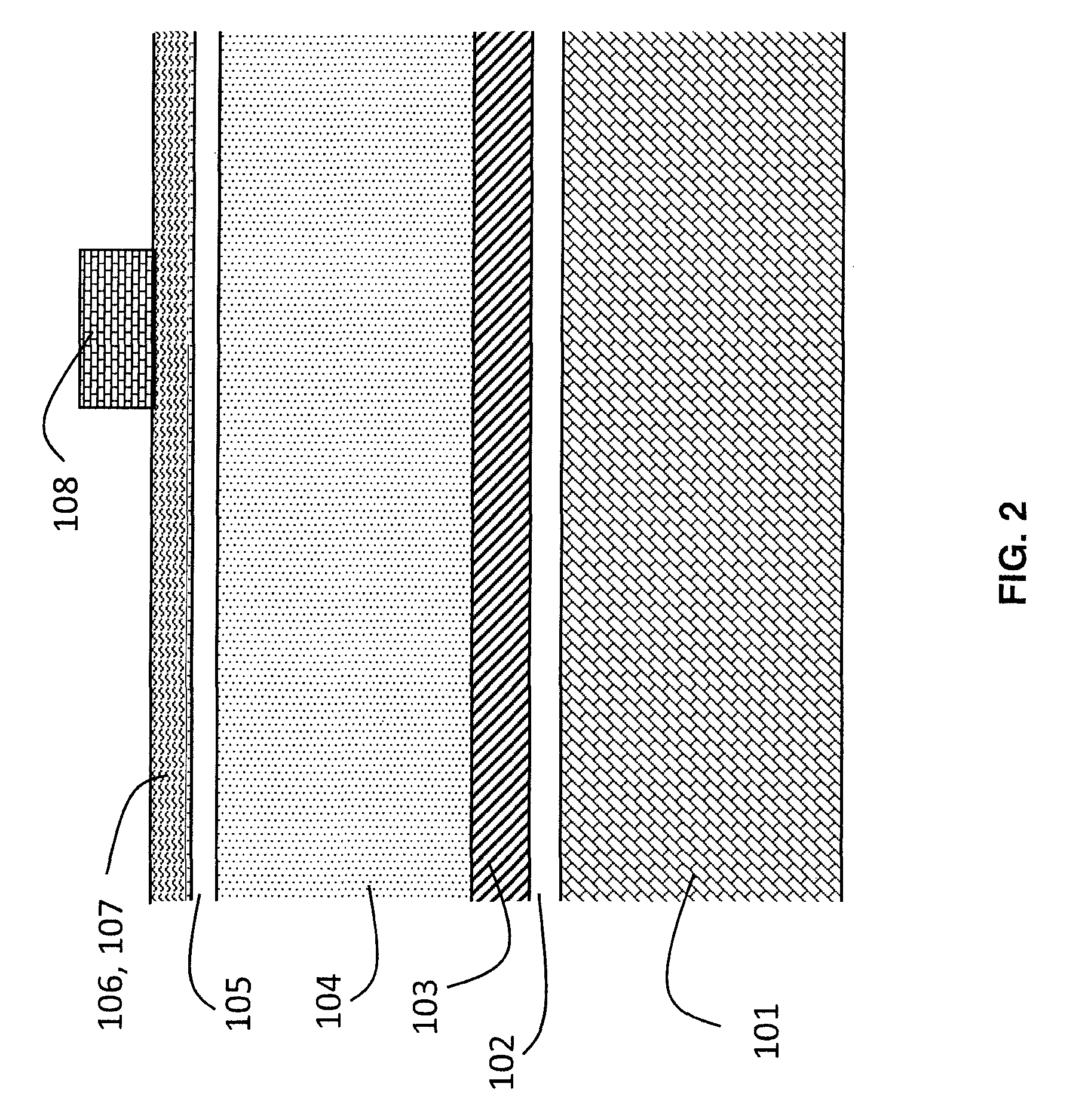
[0014]Embodiments of the present invention will now be described in detail with reference to the drawings, which are provided as illustrative examples of the invention so as to enable those skilled in the art to practice the invention. Notably, the figures and examples below are not meant to limit the scope of the present invention to a single embodiment, but other embodiments are possible by way of interchange of some or all of the described or illustrated elements. Moreover, where certain elements of the present invention can be partially or fully implemented using known components, only those portions of such known components that are necessary for an understanding of the present invention will be described, and detailed descriptions of other portions of such known components will be omitted so as not to obscure the invention. In the present specification, an embodiment showing a singular component should not be considered limiting; rather, the invention is intended to encompass ...


PUM


Abstract

Passivated emitter rear local epitaxy (PERL-e) thin Si solar cells may be formed with a heavily doped epitaxial back surface field (BSF) layer, which is patterned to form well spaced point contacts to the silicon base on the rear of the solar cell. The back side of the cell may be finished with a dielectric passivation layer and a metallization layer for making electrical contact to the cell. PERL-e thick Si solar cells may be formed with heavily doped epitaxial films as the back point contacts, where the point contacts are defined by the provision of a selectively patterned thermal oxide on the rear wafer surface. Furthermore, absorption of longer wavelength, infrared (IR), light in thin silicon solar cells may be improved by the addition of a dielectric stack on the rear surface of the solar cell (a back reflector).

Description

[0001]This application claims the benefit of U.S. Provisional Application Ser. No. 61 / 403,962 filed Sep. 22, 2010, incorporated by reference in its entirety herein.FIELD OF THE INVENTION[0002]The present invention relates generally to solar cells, and more particularly to solar cells with high efficiency.BACKGROUND[0003]The highest efficiency (24.7%) crystalline silicon solar cell produced to date is the PERL (Passivated Emitter Rear Locally diffused) cell first developed by Martin Green et al. See IEEE Transactions on Electron Devices Vol. 46, No. 10, October 1999. However, these cells are costly to fabricate since expensive float zone silicon was utilized for the device fabrication and the use of photolithography for metal contact formation is not conducive to low manufacturing cost. There is a need for lower cost solar cells with comparable efficiency to the PERL cell, and improved methods of fabricating these cells that does not involve the high temperature diffusion of boron fo...

Claims


Application Information

Patent Timeline
Patent Type & Authority Patents(United States)
IPC IPC(8): H01L21/00
CPCH01L21/00H01L31/022433H01L31/02167H01L31/02168H01L31/022425H01L31/028H01L31/03682H01L31/056H01L31/1804H01L31/1868Y02E10/52Y02E10/547Y02P70/50
Inventor RAVI, KRAMADHATI V.RAVI, TIRUNELVELI S.
Owner SVAGOS TECHNICK INC
Why Eureka
Try Eureka