Semiconductor device

a technology of semiconductor devices and semiconductors, applied in semiconductor devices, semiconductor/solid-state device details, electrical apparatus, etc., can solve the problems of short-channel effect and likely short-channel effect, and achieve high reliability, suppress the occurrence of short-channel effect due to miniaturization, and stable electrical characteristics

Inactive Publication Date: 2014-08-19
SEMICON ENERGY LAB CO LTD
View PDF178 Cites 30 Cited by
  • Summary
  • Abstract
  • Description
  • Claims
  • Application Information

AI Technical Summary

Benefits of technology

[0008]Miniaturization has been a road map for technical development in the technical field of semiconductor devices, and thus, the technical field of the semiconductor devices has been developed. As the semiconductor devices have become miniaturized, higher speed operation and lower power consumption have been achieved so far.

Problems solved by technology

However, when a transistor is miniaturized, the problem of a short-channel effect arises.
The short-channel effect is likely to occur particularly in a transistor including an oxide semiconductor because it is difficult to control the threshold voltage of such a transistor by doping, unlike a transistor including silicon.

Method used


Image

  • Semiconductor device
  • Semiconductor device
  • Semiconductor device

Examples


embodiment 1

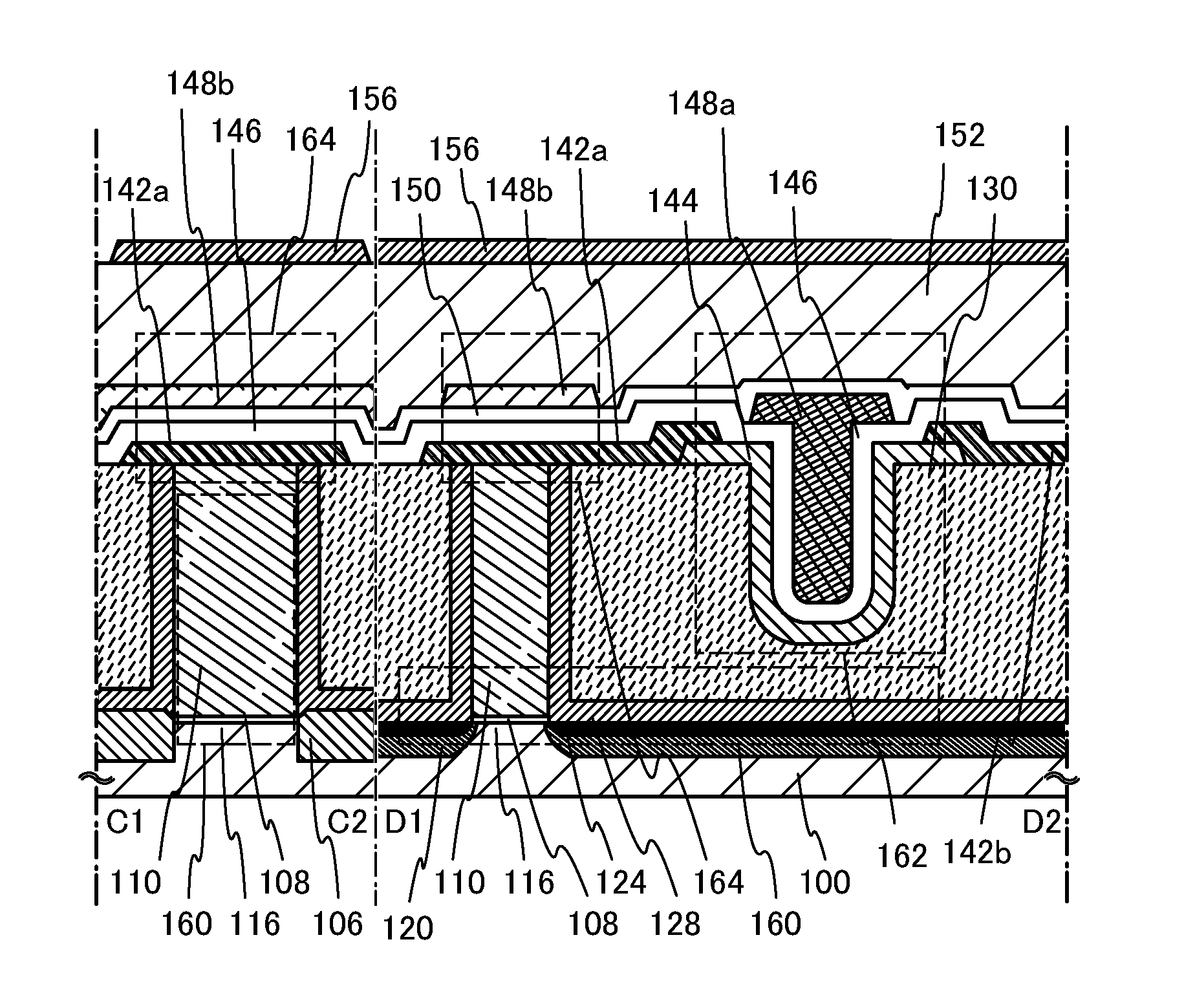
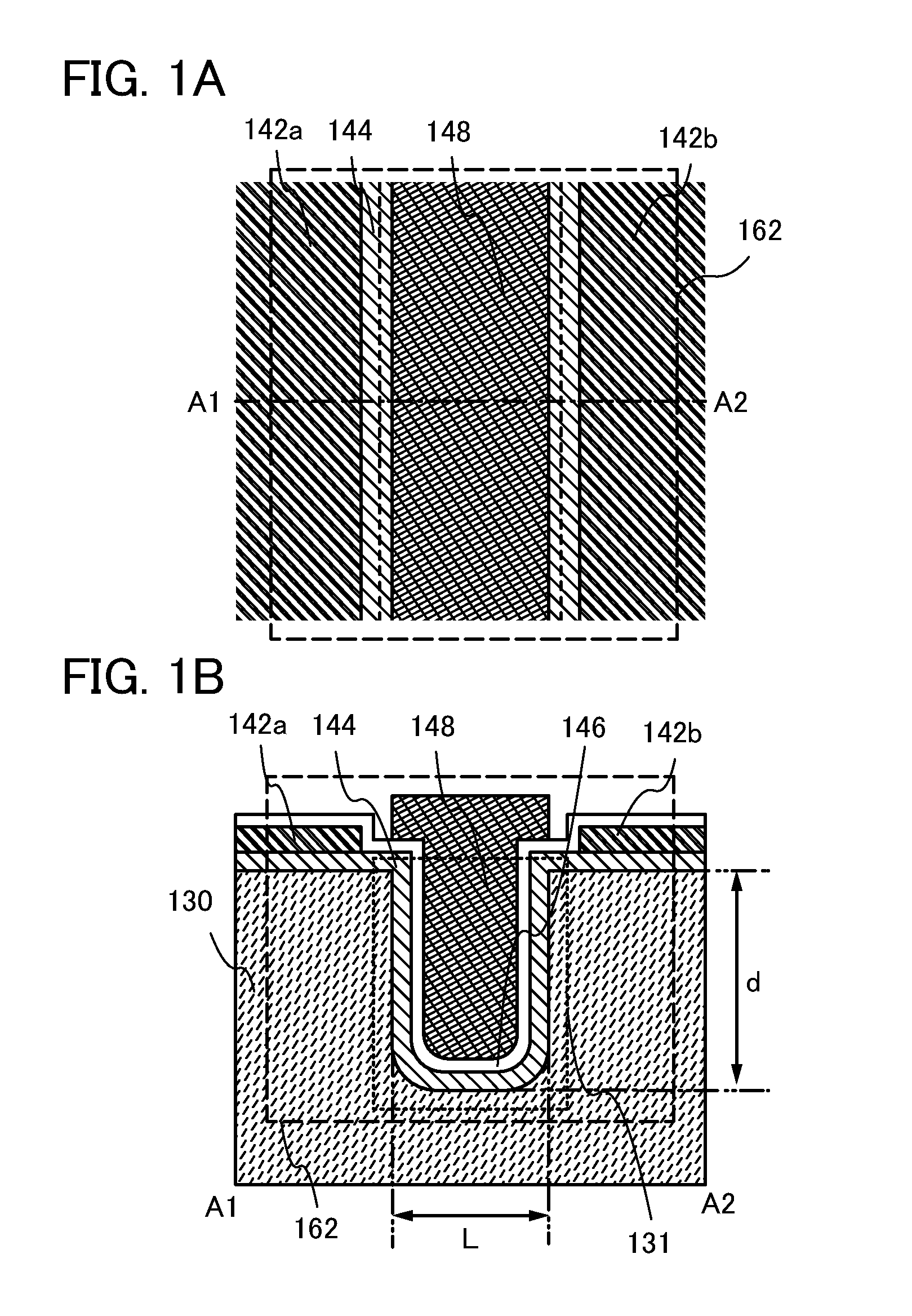
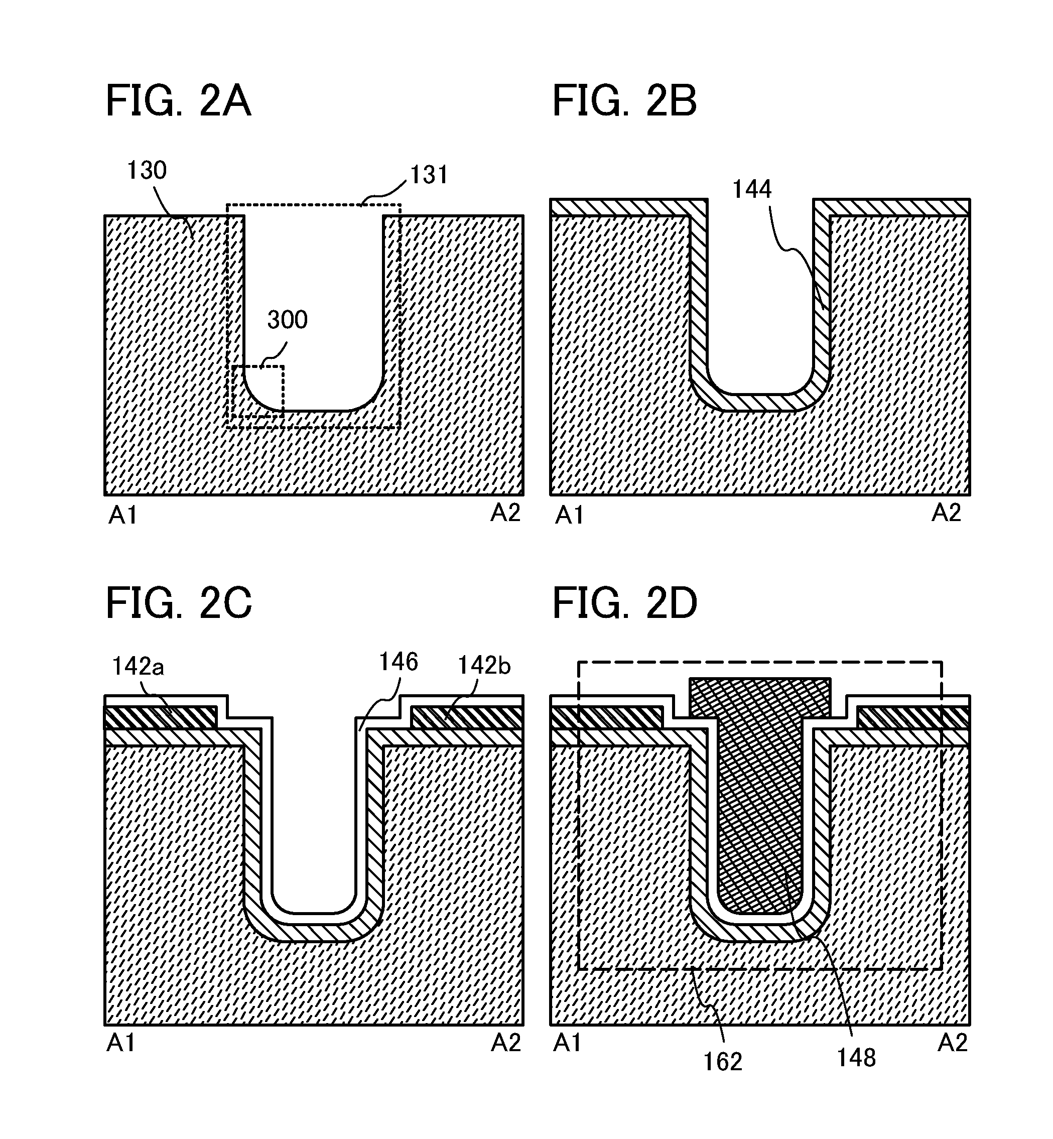
[0045]In this embodiment, one embodiment of a semiconductor device and a method for manufacturing the semiconductor device will be described with reference to FIGS. 1A and 1B, FIGS. 2A to 2D, FIGS. 12A to 12C, FIGS. 13A to 13C, and FIGS. 14A to 14C. In this embodiment, a transistor including an oxide semiconductor film will be described as an example of the semiconductor device. FIG. 1A is a plan view of a transistor 162, and FIG. 1B is a cross-sectional view taken along a dashed line A1-A2 in FIG. 1A and is an example of a cross-sectional view of the transistor 162 in the channel-length (L) direction.

[0046]As illustrated in FIGS. 1A and 1B, the transistor 162 includes an insulating layer 130 provided with a trench 131, a crystalline oxide semiconductor film 144, a gate insulating layer 146, an electrode layer 142a and an electrode layer 142b functioning as a source electrode layer and a drain electrode layer, and a gate electrode layer 148. Although not illustrated, the transistor ...

embodiment 2

[0114]In this embodiment, another embodiment of a method for manufacturing a semiconductor device will be described with reference to FIGS. 3A to 3D. The same portions as those in the above embodiment or the portions having functions similar to those in the above embodiment can be formed in manners similar to those of the above embodiment. The same steps as those in the above embodiment and steps similar to those in the above embodiment can be conducted in manners similar to those of the above embodiment. Therefore, the descriptions thereof are not repeated in this embodiment. In addition, detailed description of the same portions is omitted.

[0115]In this embodiment, an example of a method for manufacturing a semiconductor device according to the disclosed invention is described, in which an amorphous oxide semiconductor film is at least partially crystallized through heat treatment so that a crystalline oxide semiconductor film is formed which includes a crystal having a c-axis sub...

embodiment 3

[0137]In this embodiment, an example of a semiconductor device which includes the transistor 162 described in Embodiment 1 or 2, which can hold stored data even when not powered, and which has an unlimited number of write cycles will be described with reference to drawings. Note that the transistor 320 or the transistor 330 described in Embodiments 1 or 2 can also be used in the semiconductor device of this embodiment.

[0138]Since the off-state current of the transistor 162 is small, stored data can be held for a long time owing to such a transistor. In other words, it is possible to obtain a semiconductor memory device which does not require refresh operation or has an extremely low frequency of the refresh operation, which leads to a sufficient reduction in power consumption.

[0139]FIGS. 5A to 5C illustrate an example of a configuration of the semiconductor device. FIG. 5A is a cross-sectional view of the semiconductor device, FIG. 5B is a plan view of the semiconductor device, and ...


PUM


Abstract

Stable electric characteristics and high reliability are provided to a miniaturized and integrated semiconductor device including an oxide semiconductor. In a transistor (a semiconductor device) including an oxide semiconductor film, the oxide semiconductor film is provided along a trench (groove) formed in an insulating layer. The trench includes a lower end corner portion having a curved shape with a curvature radius of longer than or equal to 20 nm and shorter than or equal to 60 nm, and the oxide semiconductor film is provided in contact with a bottom surface, the lower end corner portion, and an inner wall surface of the trench. The oxide semiconductor film includes a crystal having a c-axis substantially perpendicular to a surface at least over the lower end corner portion.

Description

BACKGROUND OF THE INVENTION[0001]1. Field of the Invention[0002]An embodiment of the present invention relates to a semiconductor device and a method for manufacturing the semiconductor device.[0003]In this specification, a semiconductor device generally means a device which can function by utilizing semiconductor characteristics, and an electro-optical device, a semiconductor circuit, and an electronic device are all semiconductor devices.[0004]2. Description of the Related Art[0005]Attention has been focused on a technique for forming a transistor using a semiconductor thin film formed over a substrate having an insulating surface (also referred to as thin film transistor (TFT)). The transistor is applied to a wide range of electronic devices such as an integrated circuit (IC) or an image display device (display device). A silicon-based semiconductor material is widely known as a material for a semiconductor thin film applicable to a transistor. As another material, an oxide semic...

Claims


Application Information

Patent Timeline
Patent Type & Authority Patents(United States)
IPC IPC(8): H01L29/10
CPCH01L23/564H01L27/1225H01L29/045H01L29/7869H01L27/1156H01L29/4236H01L2924/0002H10B41/70H01L2924/00H01L29/1037H01L29/78603H10B99/00H01L21/02565H01L21/02592H01L21/02667H01L29/24H01L29/42384H01L29/51H01L29/66969H01L29/78696
Inventor ISOBE, ATSUOSASAKI, TOSHINARI
Owner SEMICON ENERGY LAB CO LTD
Why Eureka
Try Eureka