Light emitting diode and light emitting device

a technology of light emitting diodes and light emitting devices, which is applied in the field of semiconductors, can solve the problems of low luminous efficiency, short service life, and low efficiency of conventional led devices, and achieve the effects of reducing auger recombination, improving internal quantum efficiency of led, and reducing current density

Inactive Publication Date: 2014-08-19
ENRAYTEK OPTOELECTRONICS
View PDF29 Cites 2 Cited by
  • Summary
  • Abstract
  • Description
  • Claims
  • Application Information

AI Technical Summary

Benefits of technology

[0006]It is an object of this invention to provide an LED with high luminous efficiency.
[0010]In comparison with conventional technologies, the present invention has the following advantages:
[0011]1. The contact holes formed on the backface of the substrate electrically connect the n-type GaN semiconductor layer, which reduces the current density, thus reducing the auger recombination and improving the internal quantum efficiency of the LED;
[0012]2. The side walls of the pyramid-shaped recesses formed on the upper surface of the substrate reflect light emitted form the LED chip to the light-exiting surface of the LED, which increases the area of reflecting surface and improves the luminous efficiency of the LED.

Problems solved by technology

However, conventional LED devices have a problem of low luminous efficiency, which are only several percentage points before LED packaging.
A large amount of energy is wasted inside LED devices, causing both energy waste and shorter service life.
However, in the method, a film structure including stacked high refractive index layers and low refractive index layers is required to be formed on a substrate.
Therefore, the manufacture process of the method is complex.

Method used


Image

  • Light emitting diode and light emitting device
  • Light emitting diode and light emitting device
  • Light emitting diode and light emitting device

Examples


Embodiment Construction

[0017]Hereunder, the present invention will be described in detail with reference to embodiments, in conjunction with the accompanying drawings.

[0018]Embodiments to which the present invention is applied are described in detail below. However, the invention is not restricted to the embodiments described below.

[0019]As described in the background, in conventional technology, to improve the luminous efficiency of LED, a film structure including stacked high refractive index layers and low refractive index layers is required to be formed on a substrate, which leads to a complex manufacture process.

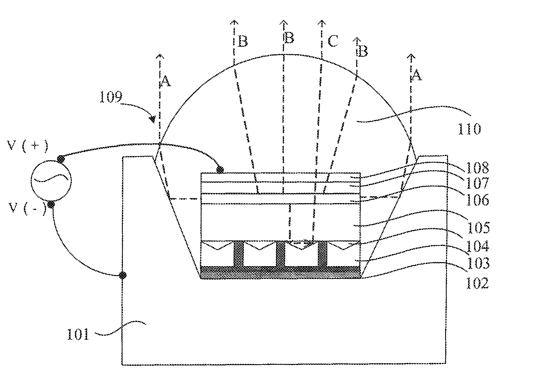
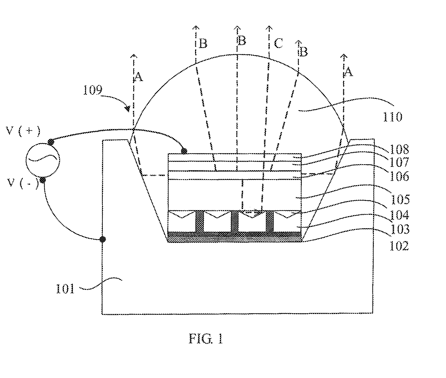
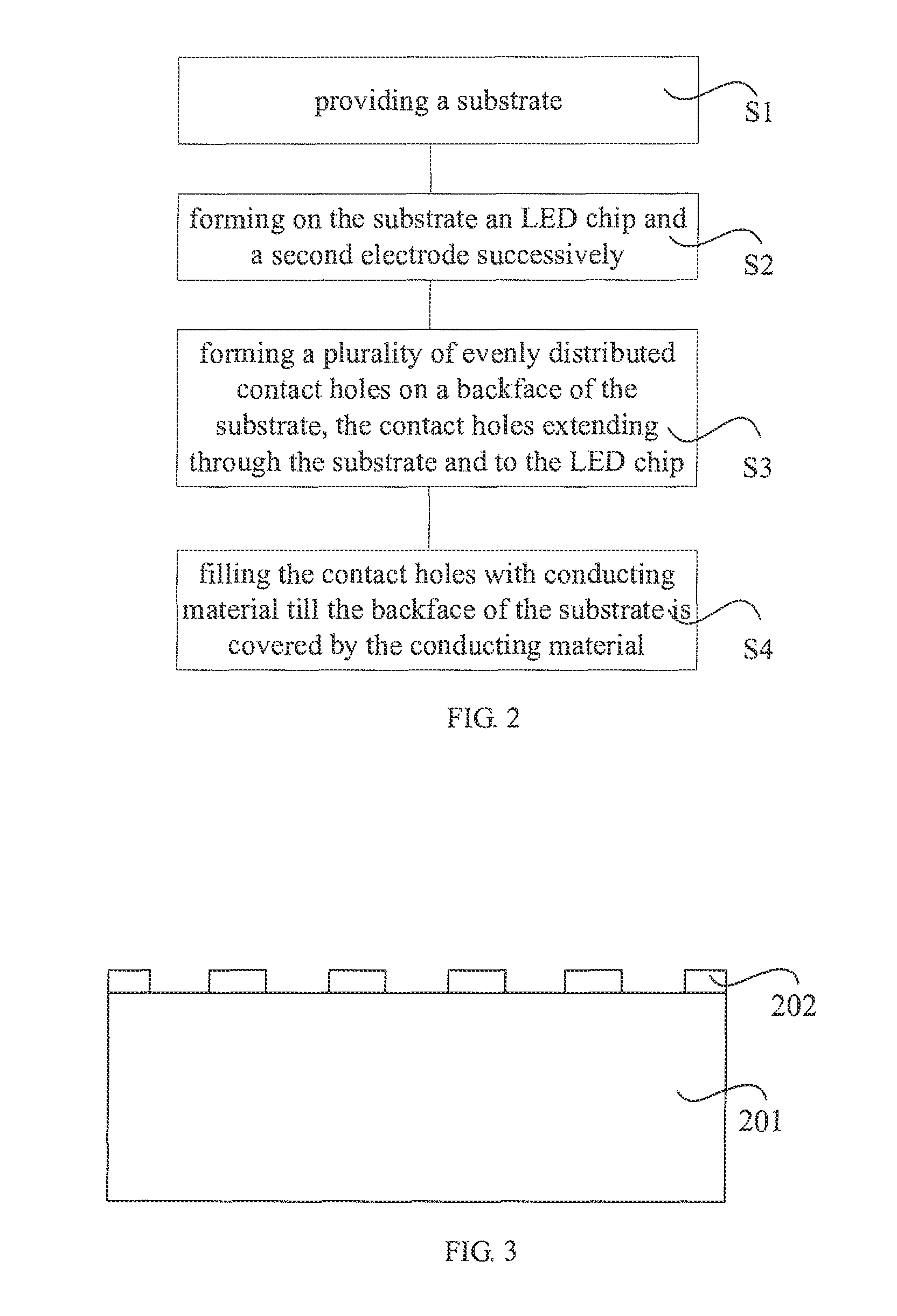
[0020]To solve the above problem, the present invention provides a light emitting device including an LED. The LED includes: a first electrode, for connecting the LED to a negative terminal of a power supply; a substrate and an LED chip successively located on the first electrode. A plurality of contact holes are formed through the substrate, the contact holes are evenly distributed and fille...


PUM


Abstract

The present invention provides an LED and the manufacturing method thereof, and a light emitting device. The LED includes a first electrode, for connecting the LED to a negative terminal of a power supply; a substrate, located on the first electrode; and an LED chip, located on the substrate; in which a plurality of contact holes are formed through the substrate, the contact holes are evenly distributed and filled with electrode plugs connecting the first electrode to the LED chip. The light emitting device includes the LED, and further includes a base and an LED mounted on the base. The manufacturing method includes: providing a substrate; forming on the substrate an LED chip and a second electrode successively; forming a plurality of evenly distributed contact holes on a backface of the substrate, the contact holes extending through the substrate and to the LED chip; and filling the contact holes with conducting material till the backface of the substrate is covered by the conducting material. The LED has a high luminous efficiency and the manufacturing method is easy to implement.

Description

[0001]The present application claims the priority of Chinese Patent Application No. 201010538397.1, entitled “Light Emitting Diode and Manufacturing Method thereof, Light Emitting Device”, and filed Nov. 9, 2010, the entire disclosure of which is incorporated herein by reference.FIELD OF INVENTION[0002]The present invention relates to the semiconductor field, and particularly relates to a light emitting diode and manufacturing method thereof and light emitting device.BACKGROUND OF THE INVENTION[0003]A light emitting diode (LED) is a semiconductor device, which emits different colored light driven by current. Semiconductor material consisting of a compound of the III-V family such as gallium nitride (GaN) has attracted widespread attention because of its wide bandgap, high luminous efficiency, high saturated electron drift velocity, high chemical stability, and huge potential in high brightness blue LED, blue lasers and other optoelectronic fields.[0004]However, conventional LED devi...

Claims


Application Information

Patent Timeline
Patent Type & Authority Patents(United States)
IPC IPC(8): H01L33/20H01L33/00H01L31/12H01L33/38H01L27/15
CPCH01L33/387H01L33/382H01L33/20H01L2933/0066H01L33/0075H01L33/0066H01L2933/0058H01L2933/0016H01L2933/0041
Inventor CHANG, RICHARD, RUGIN
Owner ENRAYTEK OPTOELECTRONICS
Why Eureka
Try Eureka