Ultra-miniaturized electron optical microcolumn

a technology of electron optical microcolumn and ultra-miniaturized electron, which is applied in the field of ultra-miniaturized electron optical microcolumn, can solve the problems of low processing speed of electron column, bulky size of electron column for generating and controlling electron beam, and defects in samples or structures of substrates, so as to improve assembly precision of products, the effect of minimizing the diameter of the probe and minimizing the alignment error of electron optical lenses generated during the fabrication of electron optical columns

Active Publication Date: 2014-09-16
IND UNIV COOP FOUND SUNMOON UNIV
View PDF10 Cites 0 Cited by
  • Summary
  • Abstract
  • Description
  • Claims
  • Application Information

AI Technical Summary

Benefits of technology

[0010]Accordingly, the present invention has been made keeping in mind the above problems occurring in the related art, and the present invention is intended to propose a ultra-miniaturized electron optical column (referred hereinafter to as an ‘electron optical microcolumn’) capable of optimizing the trajectory of electron beams and minimizing a diameter of a probe.
[0011]Another aspect of the present invention is to provide an electron optical microcolumn in which unlike a conventional electron optical column, a focusing electrode is disposed between an extraction grid (extractor or extraction electrode) and an anode grid (accelerator or acceleration electrode), thereby minimizing the size thereof.
[0012]A further aspect of the present invention is to provide an electron optical microcolumn in which unlike a conventional electron optical column, a focusing electrode is disposed between an extraction grid and an anode grid so that electron beams can be exactly focused on the surface of a target, thereby improving resolution.

Problems solved by technology

Generally, although manufacturing apparatuses and inspection apparatuses using an electron beam, which are used in semiconductor and display industries, have very high resolution compared to existing optical equipment, the size of an electron column for generating and controlling an electron beam is bulky.
Thus, the electron column using an electron beam has a large acceleration voltage ranging from a few kV to tens of kV, as well as a large size, possibly causing defects to samples or structures of a substrate.
Further, the electron column has a low processing speed and thus low productivity, so that the electron column is limited to use as a manufacturing device for a mask for a semiconductor, an inspection device for a thin film transistor (TFT) substrate for a display, or the like.
However, such a miniaturized electron column has problems that it has reduced resolution compared to the bulky electron column, due to its simple structure and low acceleration voltage, and that, in a case where a probe current to a target surface decreases, it is difficult to detect secondary electrons generated from the target surface when the target surface is scanned at high speed with an electron beam in order to increase resolution.
Further, in a case where a plurality of miniaturized electron columns are arranged in order to improve the operation performance of an assembly of the electron columns, it is difficult to precisely align the electron columns together, thereby requiring further research to develop a structure for the integration of a multiplicity of electron optical columns in a single silicon substrate.
Like this, the conventional microminiaturized electron optical column is configured such that it is composed of the source lens and the focusing lens with the octupole electrostatic double deflectors interposed therebetween, so that it is very difficult to precisely align centers of these lenses during assembly.
Further, although an error of alignment between the source lens and the focusing lens can be corrected to some extent using the arrangement of the octupole electrostatic double deflectors, in this case, the structure of the assembly becomes complicated as does the application method of drive voltage.

Method used


Image

  • Ultra-miniaturized electron optical microcolumn
  • Ultra-miniaturized electron optical microcolumn
  • Ultra-miniaturized electron optical microcolumn

Examples


Embodiment Construction

[0033]Reference will now be made in greater detail to a preferred embodiment of the invention, an example of which is illustrated in the accompanying drawings. Wherever possible, the same reference numerals will be used throughout the drawings and the description to refer to the same or like parts. In the following description, it is to be noted that, when the functions of conventional elements and the detailed description of elements related with the present invention may make the gist of the present invention unclear, a detailed description of those elements will be omitted.

[0034]A description will now be made in detail of an exemplary electron optical column (referred hereinafter to as an ‘electron optical microcolumn’) according to an embodiment of the present invention with reference to the accompanying drawings.

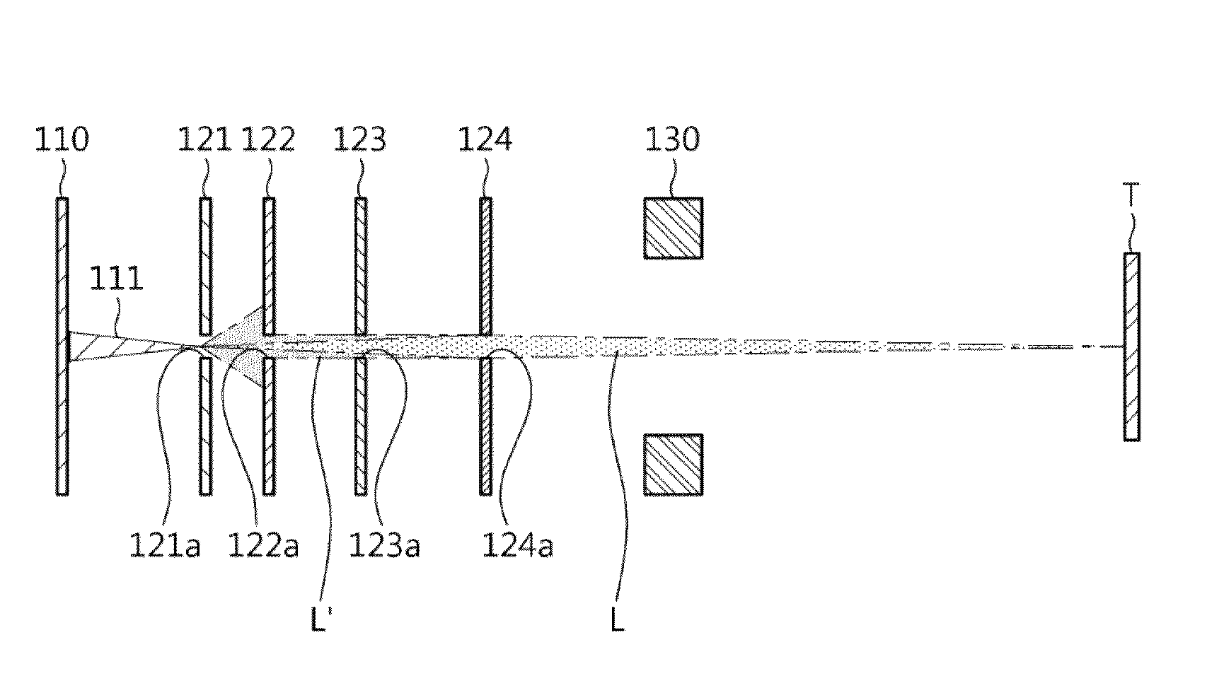
[0035]FIG. 1 is a perspective view showing a configuration of an electron optical microcolumn according to an embodiment of the present invention.

[0036]Referring to FIG...


PUM


Abstract

An ultra-miniaturized electron optical microcolumn is provided. The electron optical microcolumn includes an electron-emitting source emitting electrons using a field emission principle, an extraction electrode causing the emission of electrons from the electron-emitting source, a focusing electrode to which voltage is flexibly applied in response to a working distance to a target for regulating a focusing force of electron beams emitted from the electron-emitting source, an acceleration electrode accelerating electrons emitted by the extraction electrode, a limit electrode regulating an amount and a size of electron beams using electrons accelerated by the acceleration electrode, and a deflector deflecting electron beams towards the target.

Description

CROSS-REFERENCE TO RELATED APPLICATIONS[0001]This application claims priority to Korean Patent Application No. 10-2013-0015832 filed on Feb. 14, 2013 in the Korean Intellectual Property Office (KIPO), the entire contents of which are hereby incorporated in their entirety by reference.BACKGROUND[0002]1. Field of the Invention[0003]The present invention relates, in general, to an ultra-miniaturized electron optical microcolumn and, more particularly, to a ultra-miniaturized electron optical microcolumn which is able to be manufactured into a compact size and optimize the trajectory of an electron beam.[0004]2. Description of the Related Art[0005]Generally, although manufacturing apparatuses and inspection apparatuses using an electron beam, which are used in semiconductor and display industries, have very high resolution compared to existing optical equipment, the size of an electron column for generating and controlling an electron beam is bulky. Thus, the electron column using an el...

Claims


Application Information

Patent Timeline
Patent Type & Authority Patents(United States)
IPC IPC(8): H01J29/46H01J3/36H01J3/14H01J3/26
CPCH01J3/26H01J3/14H01J3/021H01J3/18H01J37/04H01J3/12H01J2237/1205H01J3/30H01J37/06H01J37/147
Inventor OH, TAE SIKKIM, HO SEOBKIM, DAE WOOKAHN, SEUNG-JOON
Owner IND UNIV COOP FOUND SUNMOON UNIV
Why Eureka
Try Eureka