Forming a diffusion break during a RMG process

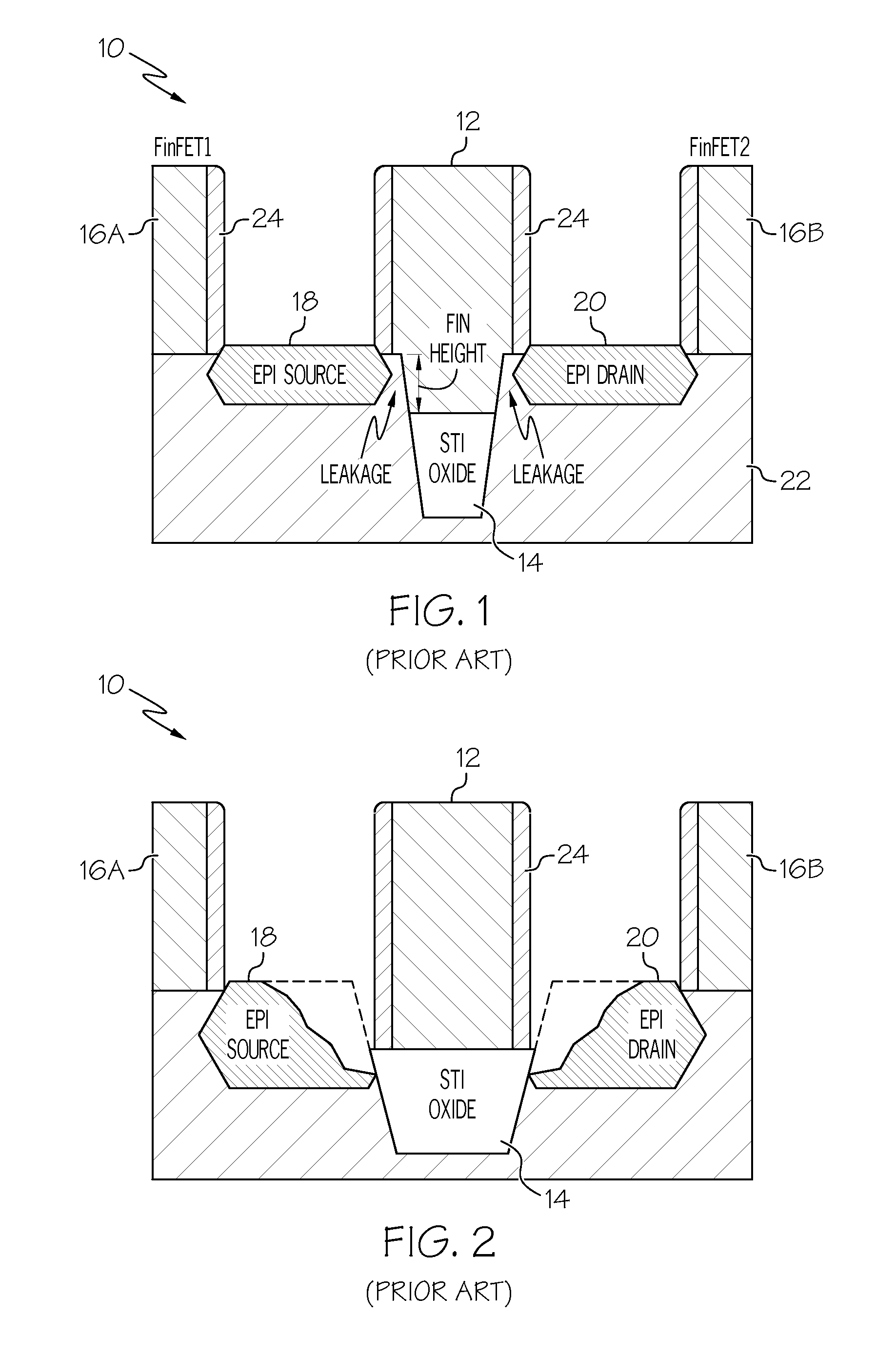
a technology of diffusion break and diffusion break, applied in the field of semiconductors, can solve the problems of current crowding, difficult to achieve the small critical dimension (cd) required for patterning isolation trenches, and inability to position the area

Active Publication Date: 2014-09-30
GLOBALFOUNDRIES US INC
View PDF1 Cites 90 Cited by
  • Summary
  • Abstract
  • Description
  • Claims
  • Application Information

AI Technical Summary

Problems solved by technology

However, patterning isolation trench 14 to reach the small critical dimensions (CD) required is difficult with conventional lithography and etch techniques available.
This is especially problematic when trying to land source and drain contacts on the epi of source 18 and drain 20.
In this case, the contact area will not be positioned as high as desired, which may result in current crowding issues.

Method used


Image

  • Forming a diffusion break during a RMG process
  • Forming a diffusion break during a RMG process
  • Forming a diffusion break during a RMG process

Examples


Embodiment Construction

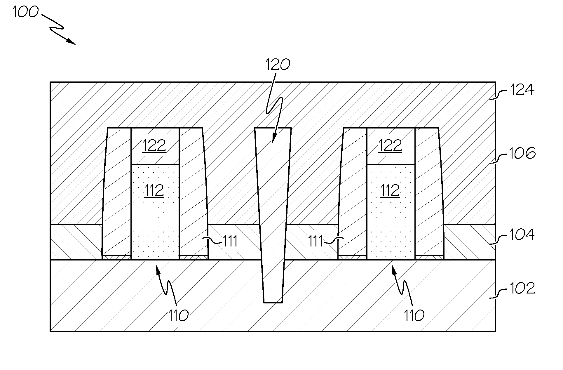
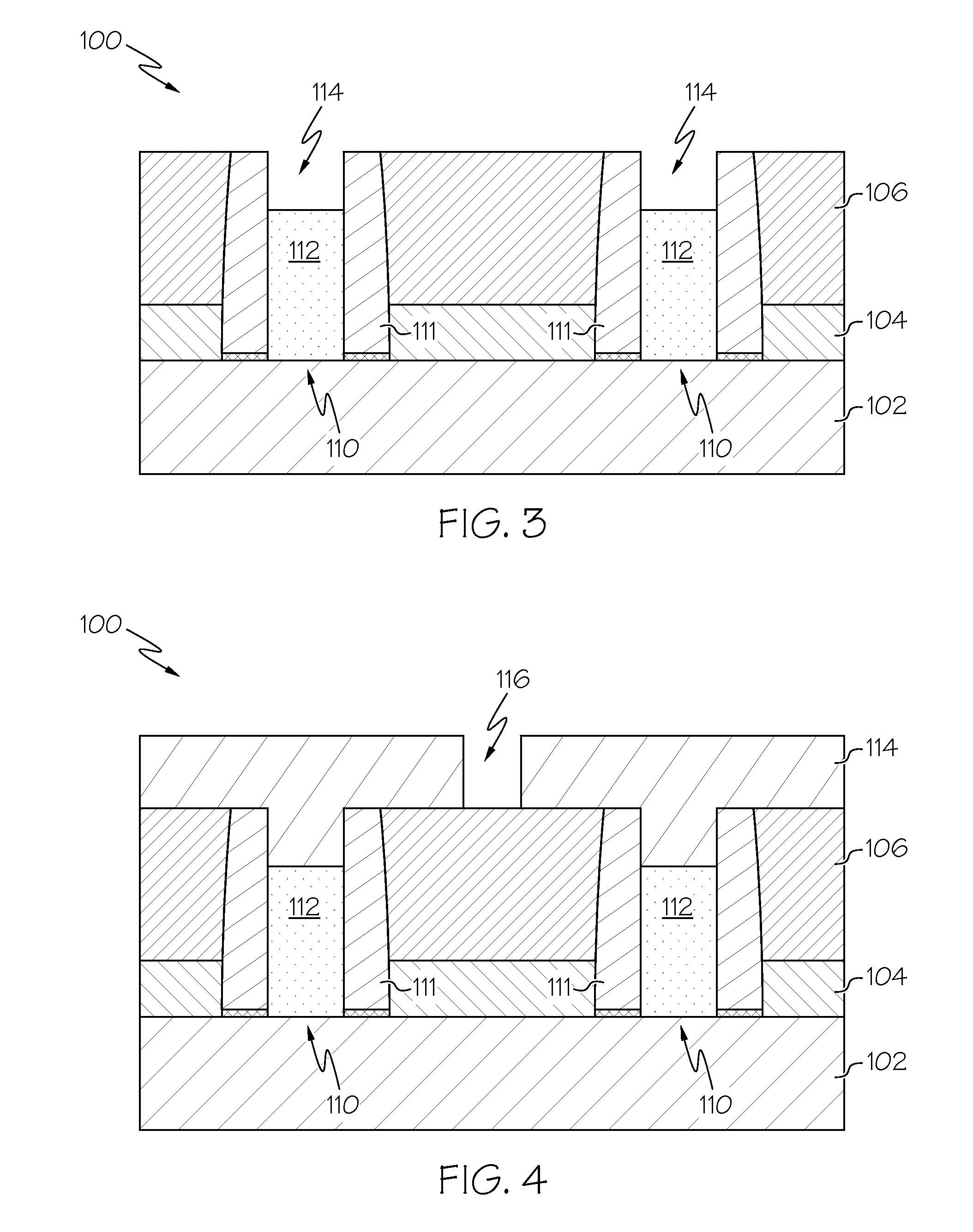
[0028]Exemplary embodiments will now be described more fully herein with reference to the accompanying drawings, in which exemplary embodiments are shown. Described are approaches forming a diffusion break during a replacement metal gate process. Specifically, a semiconductor device is provided with a set of replacement metal gate (RMG) structures over a set of fins patterned from a substrate; a dielectric material over an epitaxial junction area; an opening formed between the set of RMG structures and through the set of fins, wherein the opening extends through the dielectric material, the expitaxial junction area, and into the substrate; and silicon nitride (SiN) deposited within the opening to form the diffusion break.

[0029]It will be appreciated that this disclosure may be embodied in many different forms and should not be construed as limited to the exemplary embodiments set forth herein. Rather, these exemplary embodiments are provided so that this disclosure will be thorough ...


PUM

PropertyMeasurementUnit
structuresaaaaaaaaaa
RMG structuresaaaaaaaaaa
dielectricaaaaaaaaaa

Abstract

Embodiments herein provide approaches for forming a diffusion break during a replacement metal gate process. Specifically, a semiconductor device is provided with a set of replacement metal gate (RMG) structures over a set of fins patterned from a substrate; a dielectric material over an epitaxial junction area; an opening formed between the set of RMG structures and through the set of fins, wherein the opening extends through the dielectric material, the expitaxial junction area, and into the substrate; and silicon nitride (SiN) deposited within the opening to form the diffusion break.

Description

TECHNICAL FIELD[0001]This invention relates generally to the field of semiconductors, and more particularly, to forming a diffusion break during a replacement metal gate (RMG) process.RELATED ART[0002]A typical integrated circuit (IC) chip includes a stack of several levels or sequentially formed layers of shapes. Each layer is stacked or overlaid on a prior layer and patterned to form the shapes that define devices (e.g., field effect transistors (FETs)) and connect the devices into circuits. In a typical state of the art complementary insulated gate FET process, such as what is normally referred to as CMOS, layers are formed on a wafer to form the devices on a surface of the wafer. Further, the surface may be the surface of a silicon layer on a silicon on insulator (SOI) wafer. A simple FET is formed by the intersection of two shapes, a gate layer rectangle on a silicon island formed from the silicon surface layer. Each of these layers of shapes, also known as mask levels or layer...

Claims


Application Information

Patent Timeline
Patent Type & Authority Patents(United States)
IPC IPC(8): H01L21/76H01L21/02H01L21/762H01L29/78
CPCH01L21/76224H01L29/785H01L21/02104H01L21/823431H01L27/0886H01L29/66545H01L29/66795
Inventor PHAM, DANIELHU, ZHENYUWEI, ANDYLICAUSI, NICHOLAS V.
Owner GLOBALFOUNDRIES US INC
Why Eureka
Try Eureka