Production method for a bulk SiC single crystal with a large facet and monocrystalline SiC substrate with homogeneous resistance distribution

a monocrystalline silicon carbide and single crystal technology, applied in the direction of crystal growth process, transportation and packaging, natural mineral layered products, etc., can solve the problem of leaving the expensive substrate surface unused, and achieve the effect of improving the suitability for component production

Active Publication Date: 2014-10-21
SICRYSTAL GMBH
View PDF4 Cites 41 Cited by
  • Summary
  • Abstract
  • Description
  • Claims
  • Application Information

AI Technical Summary

Benefits of technology

[0006]It is accordingly an object of the invention to provide a production method for a bulk SiC single crystal with a large facet and a monocrystalline SiC substrate with homogeneous resistance distribution which overcome the above-mentioned disadvantages of the prior art methods and devices of this general type, which has improved suitability for component production.

Problems solved by technology

The previous inefficient practice of recessing the (previously too highly doped) facet region for the production of high-grade components, and leaving expensive substrate surface unused, is therefore superfluous.

Method used


Image

  • Production method for a bulk SiC single crystal with a large facet and monocrystalline SiC substrate with homogeneous resistance distribution
  • Production method for a bulk SiC single crystal with a large facet and monocrystalline SiC substrate with homogeneous resistance distribution
  • Production method for a bulk SiC single crystal with a large facet and monocrystalline SiC substrate with homogeneous resistance distribution

Examples


Embodiment Construction

[0041]Mutually corresponding parts are provided in FIGS. 1 to 8 with the same reference numerals. Details of the embodiments described in more detail below may represent an invention taken on their own or be part of a subject of the invention.

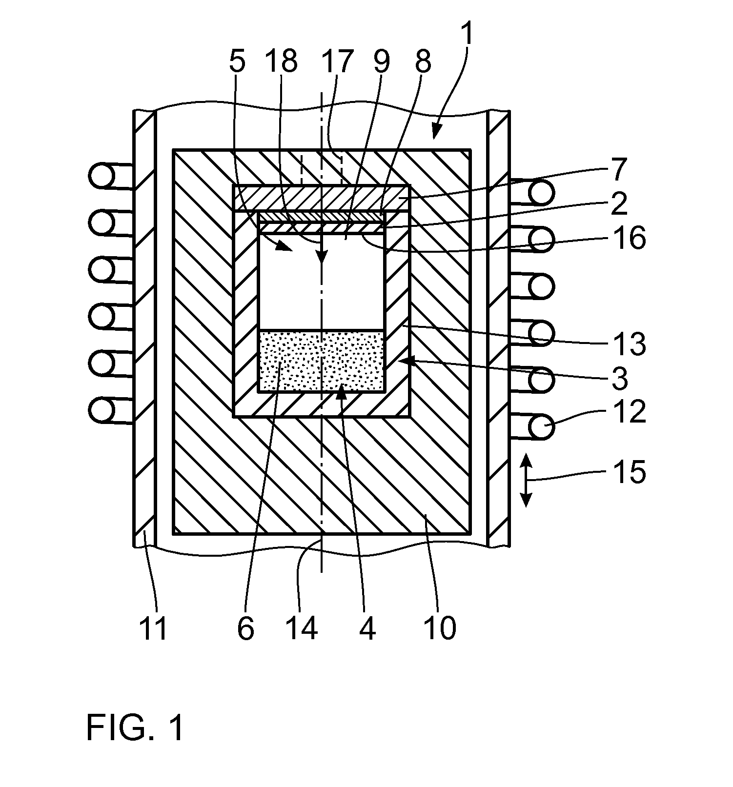
[0042]Referring now to the figures of the drawing in detail and first, particularly, to FIG. 1 thereof, there is shown an embodiment of a growth arrangement 1 for producing a bulk SiC single crystal 2 by sublimation growth. The growth arrangement 1 contains a growing crucible 3, which contains an SiC supply region 4 and a crystal growth region 5. Powdery SiC source material 6, which is poured as a pre-finished starting material before the beginning of the growth process into the SiC supply region 4 of the growing crucible 3, for example, is located in the SiC supply region 4.

[0043]A seed crystal 8 is provided on an inner wall opposing the SiC supply region 4, of the growing crucible 3, namely on its crucible lid 7, in the crystal growth region ...


PUM

PropertyMeasurementUnit
diameteraaaaaaaaaa
diameteraaaaaaaaaa
diameteraaaaaaaaaa

Abstract

A method is used to produce a bulk SiC single crystal. A seed crystal is arranged in a crystal growth region of a growing crucible. An SiC growth gas phase is produced in the crystal growth region. The bulk SiC single crystal having a central longitudinal mid-axis grows by deposition from the SiC growth gas phase, the deposition taking place on a growth interface of the growing bulk SiC single crystal. The SiC growth gas phase is at least partially fed from an SiC source material and contains at least one dopant from the group of nitrogen, aluminum, vanadium and boron. At least in a central main growth region of the growth interface arranged about the longitudinal mid-axis, a lateral temperature gradient of at most 2 K / cm measured perpendicular to the longitudinal mid-axis is adjusted and maintained in this range. The bulk SiC single crystal has a large facet region.

Description

[0001]This application claims the priority, under 35 U.S.C. §119, of German application DE 10 2010 029 756.9, filed Jun. 7, 2010; the prior application is here-with incorporated by reference in its entirety.BACKGROUND OF THE INVENTIONField of the Invention[0002]The invention relates to a method for producing a bulk SiC single crystal and a monocrystalline silicon carbide substrate.[0003]The semiconductor material silicon carbide (SiC) is used because of its outstanding physical, chemical, electrical and optical properties, inter alia also as the starting material for power electronics semiconductor components, for high-frequency components and for special light-emitting semiconductor components. SiC substrates (e.g. SiC wafers) with as large as possible a substrate diameter, quality that is as high as possible and also a specific electrical resistance which is as uniform as possible are required for these components.[0004]The basis for the SiC substrates are high-grade bulk SiC sing...

Claims


Application Information

Patent Timeline
Patent Type & Authority Patents(United States)
IPC IPC(8): B32B19/00B32B17/10C30B29/36B32B3/02C30B23/02B32B9/00
CPCC30B29/36C30B23/02Y10T428/21Y10T428/31
Inventor STRAUBINGER, THOMASVOGEL, MICHAELWOHLFART, ANDREAS
Owner SICRYSTAL GMBH
Why Eureka
Try Eureka