Multijunction solar cell employing extended heterojunction and step graded antireflection structures and methods for constructing the same

a solar cell and heterojunction technology, applied in the field of semiconductor-based photovoltaic energy converters, can solve the problems of limiting the current generation capability of single junction devices, and the performance level of practical single junction solar cells has yet to be predicted by detailed balance calculations, so as to enhance the voltage and current generation capability and increase the power output of semiconductor solar cells

Active Publication Date: 2014-11-25
MAGNOLIA SOLAR
View PDF9 Cites 10 Cited by
  • Summary
  • Abstract
  • Description
  • Claims
  • Application Information

AI Technical Summary

Benefits of technology

[0007]This invention overcomes the disadvantages of the prior art by providing a multijunction solar cell structure and method of manufacturing that includes two design elements that separately, or in combination, can increase the power output of semiconductor solar cells. When fully functionalized, an illustrative embodiment combines the two sets of design elements together to increase both the voltage and current output of multijunction solar cells. Moreover, this invention provides enhancements to both the voltage and current generating capability of the III-V multijunction photovoltaic devices.
[0009]The second design element relates to the application of antireflection layers above the active region of the device. The purpose of these antireflection structures is to maximize the number of incident photons that are directed into the device active region. In particular, multiple layers of material with index of refraction intermediate between that of the top subcell material and air can be formed on the top most device surface facing the sun. These lower index of refraction layers can consist of both epitaxial semiconductor material and optical thin film material. The exact thickness and index of refraction of the layer in the antireflection structure can be adjusted to minimize reflection losses over a broad spectrum of photon wavelengths and angles of incidence.
[0010]Illustratively, efficient photovoltaic devices both maximize the creation and collection of photo-generated carriers and enhance the voltage at which photo-generated carriers are extracted.

Problems solved by technology

Non-radiative recombination processes along with reflection losses also limit the current generating capability of single junction devices.
Thus practical single junction solar cells have yet to reach the performance levels predicted by detailed balance calculations.

Method used


Image

  • Multijunction solar cell employing extended heterojunction and step graded antireflection structures and methods for constructing the same
  • Multijunction solar cell employing extended heterojunction and step graded antireflection structures and methods for constructing the same
  • Multijunction solar cell employing extended heterojunction and step graded antireflection structures and methods for constructing the same

Examples


Embodiment Construction

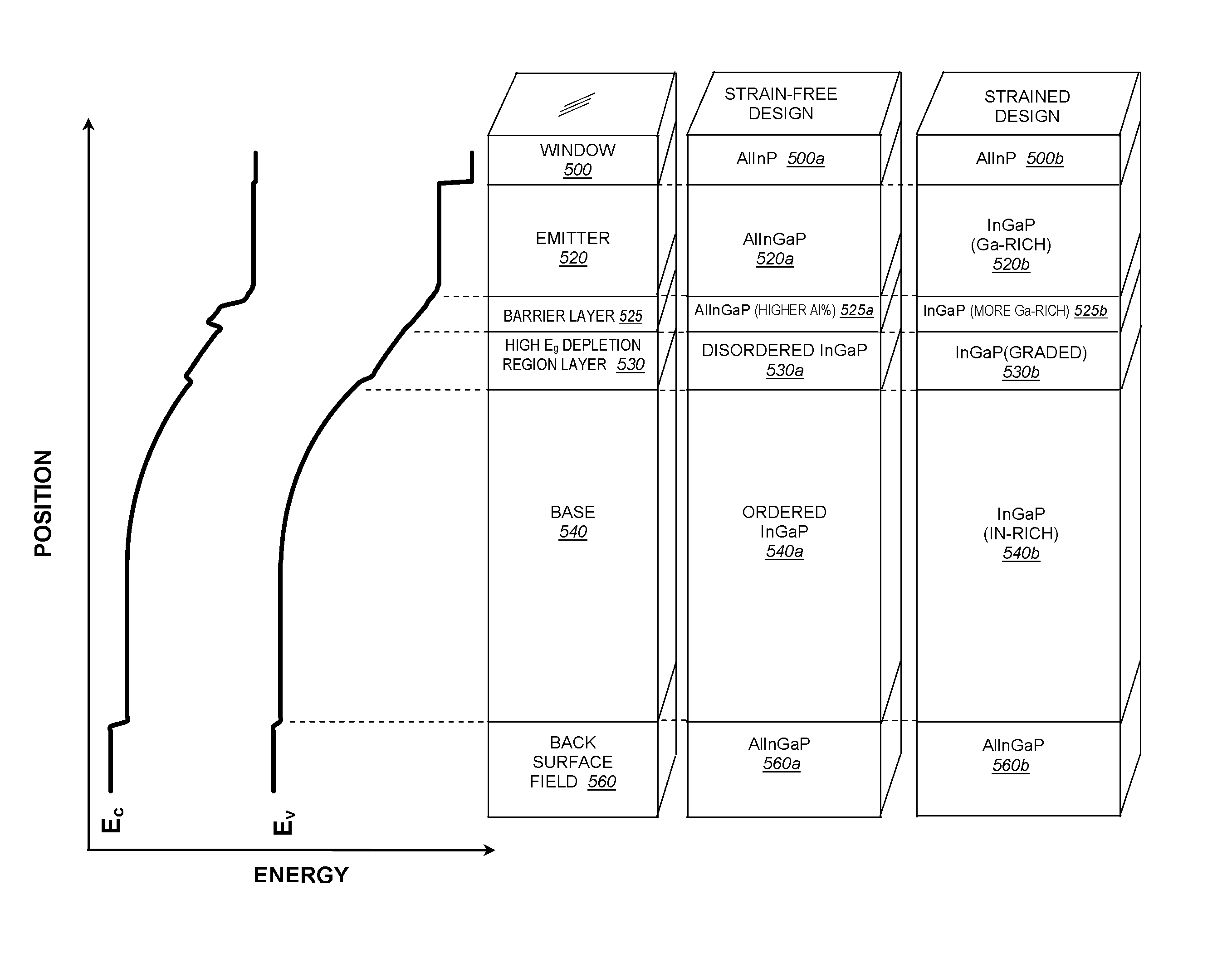
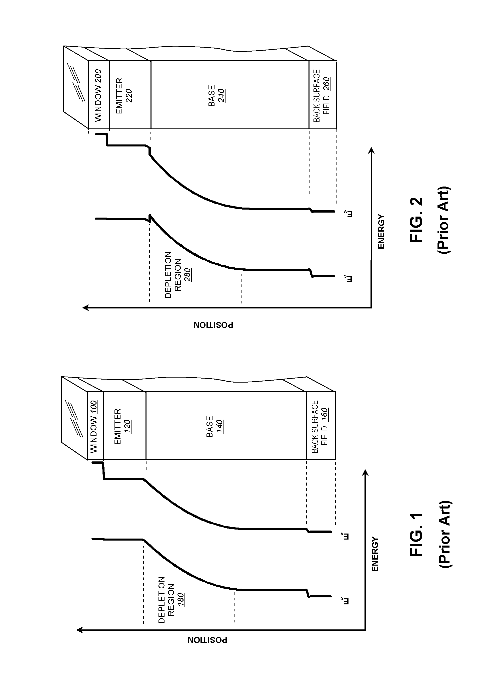
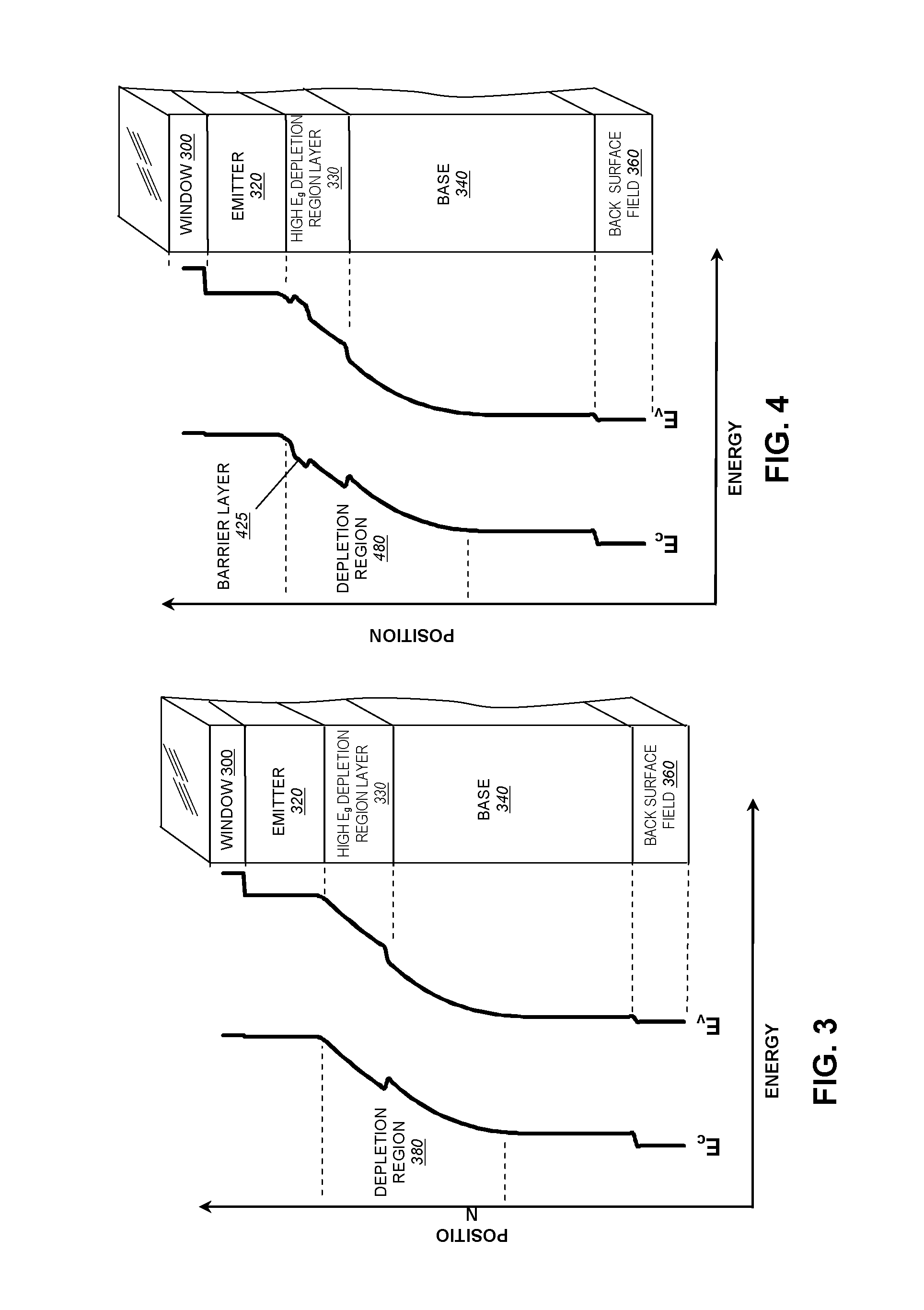
[0027]FIG. 1 details a conventional arrangement for an epitaxial subcell in a typical III-V multijunction solar cell consisting of a top window 100, an emitter 120, base 140, and back surface field layer 160. As in any PN or PIN semiconductor junction, a depletion region 180 of high electric field forms between the emitter and base layers. The window 100 and back surface field 160 layers are designed to both confine photogenerated carriers and maximize optical transmission into underlying layers. In a conventional homojunction subcell, the energy gap of emitter 120 and base 140 materials is identical, and thus the depletion region consists of a single type of semiconductor material. The depicted layers in this structure, and other layered structures depicted herein, are aligned with associated graphs of energy versus position (depth) so as to provide further understanding of the performance of the structure.

[0028]Replacing the emitter layer with a higher energy gap material and thus...


PUM


Abstract

Material and antireflection structure designs and methods of manufacturing are provided that produce efficient photovoltaic power conversion from single- and multijunction devices. Materials of different energy gap are combined in the depletion region of at least one of the semiconductor junctions. Higher energy gap layers are positioned to reduce the diode dark current and enhance the operating voltage by suppressing both carrier injections across the junction and recombination rates within the junction. Step-graded antireflection structures are placed above the active region of the device in order to increase the photocurrent.

Description

RELATED APPLICATIONS[0001]This application claims the benefit of U.S. Provisional Patent Application Ser. No. 61 / 293,469, filed on Jan. 8, 2010 entitled EFFICIENT SOLAR CELL EMPLOYING MULTIPLE ENERGY-GAP LAYERS AND LIGHT-SCATTERING STRUCTURES AND METHODS FOR CONSTRUCTING THE SAME, which is expressly incorporated herein by reference.FIELD OF THE INVENTION[0002]This invention relates to semiconductor-based photovoltaic energy converters, also known as “solar cells,” and to the design and fabrication of the same.BACKGROUND OF THE INVENTION[0003]With appropriate electrical loading, photovoltaic solid state semiconductor devices, commonly known as solar cells, covert sunlight into electrical power by generating both a current and a voltage upon illumination. The current source in a solar cell is the charge carriers that are created by the absorption of photons. These photogenerated carriers are typically separated and collected by the use of PN or PIN junctions in semiconductor materials...

Claims


Application Information

Patent Timeline
Patent Type & Authority Patents(United States)
IPC IPC(8): H01L31/065H01L31/0352H01L31/0304H01L31/0725H01L31/00
CPCG02B1/115H01L31/035263Y02E10/544H01L31/02165Y02E10/50H01L31/03046H01L31/02168H01L31/0725H01L31/065Y02E10/52H01L31/0543H01L31/0547H01L31/0232H01L31/0481H01L31/186H01L31/0445H01L31/056H01L31/0203H01L31/022425H01L31/035236H01L31/0735H01L31/184H01L31/1844H01L31/022475H01L31/048H01L31/1884
Inventor WELSER, ROGER E.SOOD, ASHOK K.
Owner MAGNOLIA SOLAR
Why Eureka
Try Eureka