Fault protector for opto-electronic devices and associated methods

a technology of opto-electronic devices and fault protectors, applied in the direction of circuit arrangements, emergency protective arrangements for limiting excess voltage/current, semiconductor lasers, etc., can solve the problems of opto-electronic device failure, product containing opto-electronic devices often seem to mysteriously fail, and most opto-electronic devices can be easily damaged, so as to avoid adding significant resistance or capacitance to the laser diode, and to avoid the effect of com

Active Publication Date: 2014-12-02
BENNER JR WILLIAM R
View PDF13 Cites 2 Cited by
  • Summary
  • Abstract
  • Description
  • Claims
  • Application Information

AI Technical Summary

Benefits of technology

[0032]The device of the current invention advantageously overcomes the problems of previously known techniques by preventing the reverse-bias voltage from exceeding the absolute maximum specified by the laser diode manufacturer, preferably under all circumstances. It also prevents ESD or other power-related faults from exceeding (and in many cases, even reaching) the maximum forward-bias voltage of the laser diode. The invention is able to do this while not adding significant resistance or capacitance to the laser diode, thereby not complicating the task of driving the laser diode.
[0035]There are known laser diode driver configurations in which the anode of the laser diode is connected to ground and the drive current is applied to the cathode, other configurations in which the cathode of the laser diode is connected to ground and the drive current is applied to the anode, and still other configurations in which neither terminal of the laser diode is connected to ground, but rather is floating in between current monitor circuits, or even in between other laser diodes within a series string. Since the device of the present invention is connected directly across the terminals of the laser diode itself, it is able to protect the laser diode, regardless of the driver configuration or grounding orientation.

Problems solved by technology

Most opto-electronic devices can be easily damaged if their nominal voltage or current parameters are exceeded.
In fact, products that contain opto-electronic devices often seem to mysteriously fail, with no apparent provocation.
A close examination into the failure modes of these devices has revealed power surges during power-up / power-down sequences and electrostatic discharge (ESD) events as two major causes of opto-electronic device failure.
But the manufacturer makes no guarantee or representation regarding what the operational amplifier will do between a supply voltage of 0 and 2.7 volts.
Because of this, current or voltage regulation circuits may go out of balance during power-up and power-down, and often apply an over-current or over-voltage condition to the opto-electronic device that is integrated within the product.
These over-current or over-voltage conditions may stress the opto-electronic device, such that each power-up or power-down cycle accumulates in the form of device fatigue.
Eventually, the opto-electronic device may fail from the fatigue, leading to what the user experiences as a mysterious failure.
Electrostatic discharge (ESD) may also cause mysterious device failures, and there are many ways in which ESD might come in contact with a product.
When an opto-electronic device that is designed to operate with a terminal voltage of 2.2 volts experiences an ESD discharge of thousands of volts, the result can be destructive.
Laser diodes typically fail as the result of two distinct damage mechanisms.
When this occurs, the mirrored surface permanently loses its reflectivity, and the laser diode no longer functions properly.
The second damage mechanism is related to failure of a laser diode's PN junction itself.
A severe over-current or over-voltage power surge can cause localized heating and other harmful phenomena, which, under extreme conditions, can actually fracture the laser diode die.
Obviously, when this happens, the laser diode will no longer function.
Both of these damage mechanisms can be provoked by an over-voltage or over-current condition.
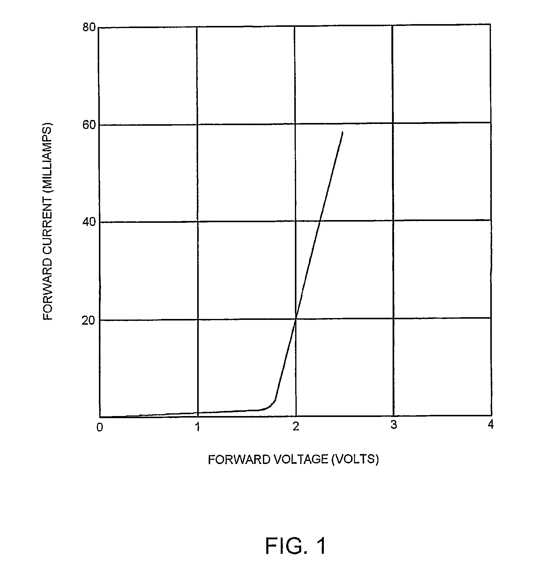
Once the maximum design current for a particular laser diode is reached (which is around 35 milliamps and 2.4 volts for this laser diode), further increases in current will likely result in failure, caused by one or both of the damage mechanisms described above.
In most cases, a low-power laser diode will be destroyed if the absolute maximum ratings are exceeded, even for a brief period of time.
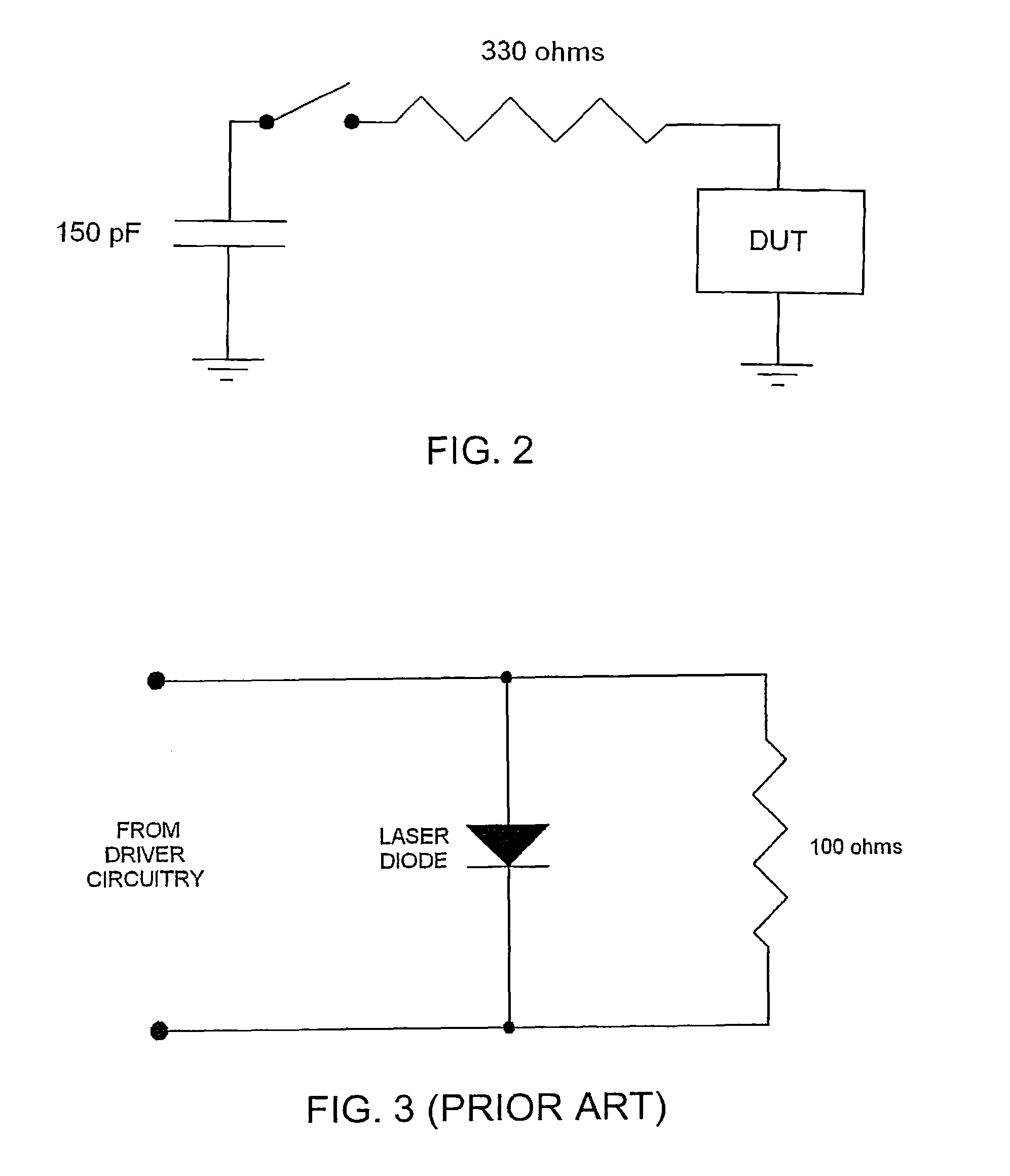
Using the human body model in FIG. 1 as a guide, it is easy to see that this protection means will not be effective.
Since this is far in excess of the typical 2.2-volt lasing threshold or 2.0-volt maximum reverse bias voltage, this would almost surely destroy the laser diode.
Although it might seem that the 100-ohm resistor could simply be replaced with a 44-milliohm resistor, this is not practical, because it would mean that, during operation, far more power would be expended in the operation of the protection resistor than the laser diode itself.
However, in real life, there are no capacitors known to exist that have purely capacitive characteristics.
All known real-world electrical components have parasitic properties.
However, even if a perfect capacitor were used that would be effective at protecting the laser diode against ESD, such a capacitance makes direct modulation of a laser diode increasingly difficult, especially at high modulation frequencies.
Thus, there are clear drawbacks to this simple capacitive approach.
However, there are several problems with this technique.
First of all, most Schottky diodes were not designed to handle nanosecond pulses of up to 50 amps.
Therefore, if the device that is put in place as the ESD protection means is destroyed by the ESD event, this is deemed to be an ineffective ESD protection means.
Second, and more important, such a configuration would only protect the laser diode from negative-ESD events (i.e., those events that would tend to reverse-bias the laser diode).
Thus, at best, a Schottky diode is an incomplete ESD protection means.
There are several problems with this technique.
One problem is that Zener diodes are notoriously slow devices, and are not able to react to nanosecond-level pulses that can be seen during ESD events.
The second, and more serious, problem is that it is believed to be impossible to choose a Zener voltage that is close enough to the forward-bias lasing threshold of the laser diode, and whose Zener voltage would track the laser diode's lasing threshold voltage throughout temperature ranges likely to be experienced by a laser diode.
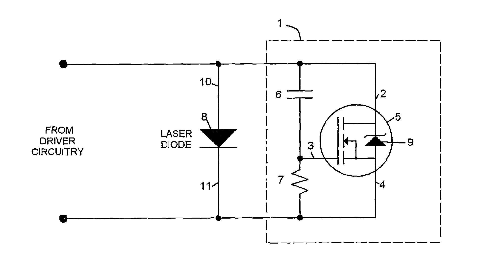
However, this “switch” approach has several important drawbacks, which will be discussed separately for the case of the relay and for the depletion-mode MOSFET.
Repeated ESD events could lead to fretting corrosion of the relay contacts, and eventual failure of the relay.
Thus, even if the laser diode itself were protected, ESD could prove destructive to the laser diode drive circuitry.
Unfortunately, the typical on-resistance of a depletion-mode MOSFET is in the range of several ohms.
Thus, a depletion-mode MOSFET would not be an effective ESD protection means for 15,000-volt ESD events.
Whether the “switch” is implemented as a relay, MOSFET, or some other device, there is another drawback to this approach.
If an ESD event happens while the laser diode is operational and lasing, the “switch” will have no effect, and will not protect the laser diode from ESD.
Therefore, this approach is not believed by the present inventor to be completely effective in preventing a low-power, fast-response laser diode from being damaged by 15,000-volt ESD.

Method used


Image

  • Fault protector for opto-electronic devices and associated methods
  • Fault protector for opto-electronic devices and associated methods
  • Fault protector for opto-electronic devices and associated methods

Examples


Embodiment Construction

[0051]The present invention will now be described more fully hereinafter with reference to the accompanying drawings, in which preferred embodiments of the invention are shown. This invention may, however, be embodied in many different forms and should not be construed as limited to the embodiments set forth herein. Rather, these embodiments are provided so that this disclosure will be thorough and complete, and will fully convey the scope of the invention to those skilled in the art.

[0052]One embodiment of the invention, as illustrated with reference to FIG. 9, is described in the context of its use to protect a laser diode from ESD and other power-related faults. One of skill in the art will recognize that the device of the present invention can be used with other opto-electronic elements, and that this usage is not intended as a limitation. The device relies on a few passive components, and a class of enhancement-mode MOSFETs that have a very low gate-to-source threshold voltage ...


PUM


Abstract

A fault protector for an opto-electronic device includes a MOSFET having an integral body-diode. A capacitor is connected between a drain and a gate of the MOSFET, and a resistor is connected between the gate and a source of the MOSFET. The drain of the MOSFET is connectable to a first terminal of an opto-electronic device, and the source of the MOSFET is connectable to a second terminal of the opto-electronic device. The device overcomes problems of previously known techniques by preventing a reverse-bias voltage from exceeding an absolute maximum specified by a manufacturer, and also prevents ESD or other power-related faults from exceeding the maximum forward-bias voltage of the laser diode, while not adding significant resistance or capacitance to the laser diode, thereby not complicating the task of driving the laser diode.

Description

FIELD OF THE INVENTION[0001]This invention is related to protecting opto-electronic devices from electrical-induced damage, such as, for example, that caused by electrostatic discharge and power surges that can occur during power-up and power-down sequences.BACKGROUND[0002]Opto-electronic devices including light emitting diodes (LEDs), laser diodes and the like, are an ever-increasing part of everyday life. Indeed, when people go through the course of a single day of their lives, they will encounter perhaps hundreds or even thousands of LEDs and laser diodes.[0003]Commonplace examples of the use of LEDs include alarm clock displays, simple indicators on consumer electronic devices, large-scale TV-like displays, and even traffic signals at street intersections. Examples of the use of laser diodes include supermarket barcode scanners, laser pointers, construction alignment devices, and police traffic radar.[0004]Most opto-electronic devices can be easily damaged if their nominal volta...

Claims


Application Information

Patent Timeline
Patent Type & Authority Patents(United States)
IPC IPC(8): H05B33/08H01S5/068H02H3/20H02H3/22H02H9/00H05B44/00
CPCH01L2924/0002Y02B20/341H01S5/06825H05B33/089Y02B20/30H01L2924/00
Inventor BENNER, JR., WILLIAM R.
Owner BENNER JR WILLIAM R
Why Eureka
Try Eureka