Method of cleaning copper material surfaces in ultra large scale integrated circuits after polishing the same

a technology of integrated circuits and copper materials, applied in the direction of detergent compounding agents, cleaning using liquids, instruments, etc., can solve the problems of long resistance and capacitance delay (rc delay), increase in later cleaning cost, and poor surface uniformity, etc., and achieve the effect of convenient operation

Inactive Publication Date: 2014-12-16
HEBEI UNIV OF TECH
View PDF9 Cites 0 Cited by
  • Summary
  • Abstract
  • Description
  • Claims
  • Application Information

AI Technical Summary

Benefits of technology

[0007]In view of the above-described problems, it is one objective of the invention to provide a method of cleaning copper material surfaces in ULSI after polishing which has an easy operation, pollution free, and cleanness.
[0021]after CMP, washing is quickly processed using the cleaning solution at a large flow rate to wash away unevenly distributed cleaning solution residues, thereby obtaining a clean and perfect surface. The surfactant quickly lowers the high surface tension of surface after polishing, reduces damaged layers, and improves the evenness of the surface. The chelating agent reacts with residues of metal ions to yield macromolecular chelates, which are washed away from the surface at large flow rate of the cleaning solution. The corrosion inhibitor forms a single molecular passive film on the surface to prevent polishing solution residues from continuing reacting with the surface, so that the perfection of the wafer surface is improved.
[0023]1) washing with cleaning solution under conditions of low pressure, large flow rate, and no time delay, not only can effectively optimize and lower the roughness of copper surface, but also can quickly wash away abrasive grains adsorbed on copper surface;
[0024]2) nonionic surfactant in the cleaning solution effectively lowers the surface tension of polishing solution residues, and at the same time prior be absorbed on copper surface to form a single molecular film which protects copper materials and avoids uneven corrosion circles on copper surface surrounding abrasive grains; and
[0025]3) cleaning solution quickly washes away polishing solution residues, thereby obtaining a clean and perfect surface.
[0026]In summary, the method has an easy operation, low cost, high efficiency, pollution free, and no additional device, prominently improves the performance of devices, and improves product yields.

Problems solved by technology

The increase in the density of integrated circuits and the decrease in the size of elements thereof make the capacity between wires and the resistance of metal interconnects enlarge, which results in longer resistance and capacitance delay (RC delay).
Therefore, grains of abrasive in the polishing solution are very easy to be adsorbed on copper surface; residues of polishing solution surrounding grains have large surface tension, and are distributed as globules on copper surface, which easily results in uneven corrosion, bad surface uniformity, increase in the later cleaning cost, and decrease in product yields.

Method used


Image

  • Method of cleaning copper material surfaces in ultra large scale integrated circuits after polishing the same
  • Method of cleaning copper material surfaces in ultra large scale integrated circuits after polishing the same
  • Method of cleaning copper material surfaces in ultra large scale integrated circuits after polishing the same

Examples


example 1

[0028]To 1912 g of 18 MΩ ultrapure deionized water, 20 g of a surfactant, 60 g of a chelating agent, and 8 g of a corrosion inhibitor were added and stirred. Subsequently, 2000 g of a cleaning solution with pH value of between 7.4 and 8.2 was collected. After alkaline CMP, copper materials were washed with the prepared cleaning solution under 3000 Pa of a low pressure and 5000 mL / min of a flow rate for 2 min, to make the surface smooth. The unevenness of the surface is 0.07, and the roughness of the surface is 0.5 nm.

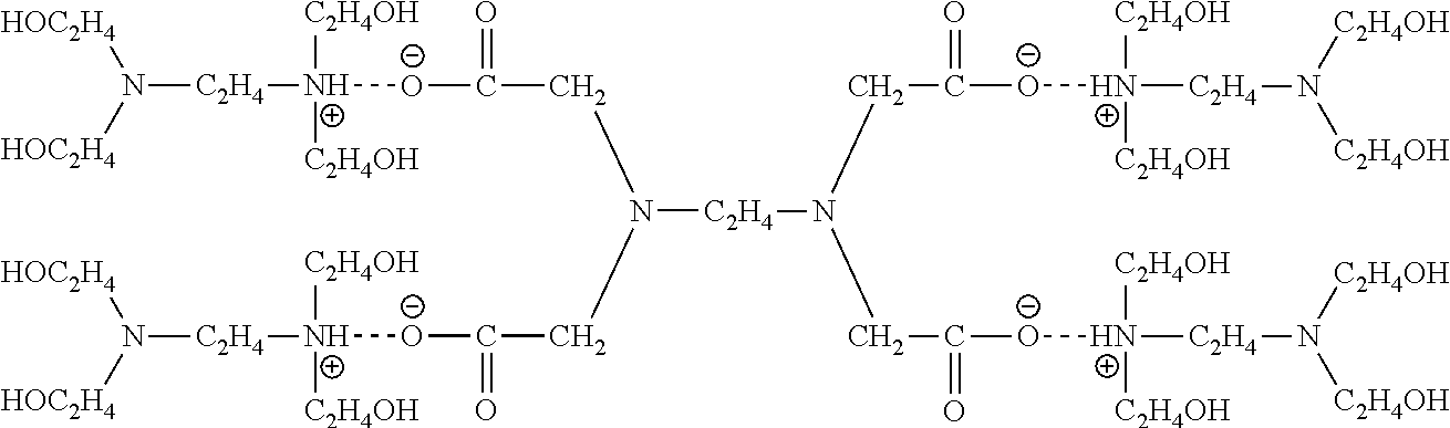
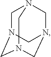
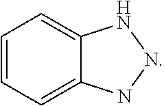
[0029]The corrosion inhibitor is an FA / O II corrosion inhibitor; the chelating agent is an FA / O II chelating agent; the surfactant is an FA / O I surfactant, Oπ-7 ((C10H21—C6H4—O—CH2CH2O)7—H), Oπ-10 ((C10H21—C6H4—O—CH2CH2O)10—H), O-20 (C12-18H25-37—C6H4—O—CH2CH2O)70—H), or (JFC). The FA / O I surfactant, the FA / O II chelating agent, and the FA / O II corrosion inhibitor all are supplied by Tianjin Jingling Microelectronics Materials Co., Ltd.

example 2

[0030]To 2745 g of 18 MΩ ultrapure deionized water, 110 g of a surfactant, 15 g of a chelating agent, and 130 g of a corrosion inhibitor were added and stirred. Subsequently, 3000 g of a cleaning solution with pH value of between 7.4 and 8.2 was collected. After alkaline CMP, copper materials were washed with the prepared cleaning solution under 2000 Pa of a low pressure and 1000 mL / min of a flow rate for 1 min, to make the surface smooth. The unevenness of the surface is 0.04, and the roughness of the surface is 0.2 nm.

[0031]Selections of the surfactant, chelating agent, and corrosion inhibitor all are same as those of Example 1.

example 3

[0032]To 3320 g of 18 MΩ ultrapure deionized water, 90 g of a surfactant, 35 g of a chelating agent, and 115 g of a corrosion inhibitor were added and stirred. Subsequently, 3560 g of a cleaning solution with pH value of between 7.4 and 8.2 was collected. After alkaline CMP, copper materials were washed with the prepared cleaning solution under 2500 Pa of a low pressure and 3000 mL / min of a flow rate for 1 min, to make the surface smooth. The unevenness of the surface is 0.05, and the roughness of the surface is 0.3 nm.

[0033]Selections of the surfactant, chelating agent, and corrosion inhibitor all are same as those of Example 1.


PUM

PropertyMeasurementUnit
pressureaaaaaaaaaa
pressureaaaaaaaaaa
flow rateaaaaaaaaaa

Abstract

A method of cleaning copper material surfaces in ultra large scale integrated circuits after polishing, the method including: a) mixing and stirring between 1 and 4 wt. % of a surfactant, between 0.5 and 3 wt. % of a chelating agent, between 0.1 and 5 wt. % of a corrosion inhibitor, and deionized water, to yield a water soluble cleaning solution with pH value of between 7.4 and 8.2; and b) washing the copper material surfaces using the cleaning solution after alkaline chemical-mechanical polishing under following conditions: between 2000 and 3000 Pa of pressure; between 1000 and 5000 mL / min of flow rate; and at least between 0.5 and 2 min of washing time.

Description

CROSS-REFERENCE TO RELATED APPLICATIONS[0001]This application is a continuation-in-part of International Patent Application No. PCT / CN2010 / 080474 with an international filing date of Dec. 30, 2010, designating the United States, now pending, and further claims priority benefits to Chinese Patent Application No. 201010232260.3 filed Jul. 21, 2010. The contents of all of the aforementioned applications, including any intervening amendments thereto, are incorporated herein by reference. Inquiries from the public to applicants or assignees concerning this document or the related applications should be directed to: Matthias Scholl P.C., Attn.: Dr. Matthias Scholl Esq., 14781 Memorial Drive, Suite 1319, Houston, Tex. 77079.BACKGROUND OF THE INVENTION[0002]1. Field of the Invention[0003]The invention relates to a method of cleaning semi-conductor materials, and more particularly to a method of cleaning copper material surfaces in ultra large scale integrated circuits (hereinbelow refer to ...

Claims


Application Information

Patent Timeline
Patent Type & Authority Patents(United States)
IPC IPC(8): C11D11/00C11D1/72C11D3/33H01L21/02B08B3/08C11D3/00
CPCC11D3/33C11D3/0073B08B3/08C11D11/0047C11D1/72H01L21/02074
Inventor LIU, YULINGLIU, XIAOYANLIU, NAHE, YANGANG
Owner HEBEI UNIV OF TECH
Why Eureka
Try Eureka