Semiconductor interband lasers and method of forming

a technology of semiconductors and lasers, applied in semiconductor lasers, lasers, active medium materials, etc., can solve the problems of unsatisfactory optical loss and worse situation, and achieve the effects of high optical loss, high optical loss, and loss loss and internal efficiency

Active Publication Date: 2015-01-06
THE BOARD OF RGT UNIV OF OKLAHOMA
View PDF11 Cites 1 Cited by
  • Summary
  • Abstract
  • Description
  • Claims
  • Application Information

AI Technical Summary

Benefits of technology

[0014]Additionally, references herein to the plasmon frequency being “close” or “closer” to the lasing frequency are understood to refer to plasmon frequencies of the semiconductor materials used to form the cladding layers. For example, for an interband cascade laser where the refractive index of the active region is 3.42, and the emission wavelength is 6 μm (ω=1660 cm−1), it is desirable to adjust the doping so that the plasma frequency of the cladding layers is 500 cm−1 or higher. This makes the refractive index of the cladding layers less than 3, ensuring good mode confinement.
[0016]It should be understood that InAs has a thermal conductivity approximately 10 times higher than that of the InAs / AlSb SL. Metals that may be used for cladding such as Au and Ag have thermal conductivities that are about 100 times higher than the InAs / AlSb SL. Thus, the replacement of the SL cladding layers with doped InAs or metal layers significantly improves heat dissipation in the laser (e.g. interband cascade lasers). Also, the growth of plasmon waveguide IC laser structures by molecular beam epitaxy (MBE) without thick SL layers would be much less demanding with dramatically reduced shutter movements on many (>1000) interfaces of the SL. Other benefits with the plasmon waveguide for IC lasers are elaborated below.
[0019]Previous IC lasers with InAs / AlSb SL cladding layers have higher optical loss. For example, 11-17 cm−1 at ˜78 K and 28-35 cm−1 at high temperatures (≧270 K), as described by Soibel, et al. in “Optical gain, loss and transparency current in high performance mid-IR interband cascade lasers”, J. Appl. Phys. Vol. 101, 093104 (2007); and by Bewley, et al in “Gain, loss, and internal efficiency in interband cascade lasers emitting at λ=3.6-4.1 μm”, J. Appl. Phys, vol. 103, article 013114 (2008). One possible reason for this high optical loss is that the SL cladding layer has a refractive index (˜3.37) that is just slightly lower than the value in the cascade core region, so the laser light significantly extends into the cladding region as shown in FIG. 1 (57% and 43% for regular and SCL waveguides, respectively). The optical penetration into the SL cladding layer may even extend into the high index GaSb substrate with more optical loss when the bottom SL cladding region is not sufficiently thick (for avoiding much worse thermal dissipation). Hence, compared to IC lasers on GaSb substrates, the optical loss can be reduced in plasmon-waveguide IC lasers with much less wave penetration into the cladding regions. In addition, the plasmon-waveguide IC lasers can be grown on n+-type (1-3×1018 cm−3 available commercially) InAs substrates, which have a permittivity lower than that of the waveguide core region and can be used as an extra cladding layer. Also, the operating voltage can be reduced further for plasmon waveguide SCH IC lasers with fewer number of cascading stages. Consequently, the power consumption in plasmon waveguide IC lasers would be reduced significantly.
[0020]Therefore, plasmon waveguide IC lasers on InAs substrates can have better performance and efficient continuous wave (cw) operation with significantly improved thermal dissipation, reduced optical loss and power consumption. Another important feature is that plasmon waveguide IC lasers are believed to be able to achieve efficient cw operation in the longer wavelength (>6 μm) region without the difficulties associated with thick SL cladding layers. Electroluminescence from IC light emitting diodes (without cladding layers) has been demonstrated in 6-15 μm wavelength region. However, it is difficult for current IC lasers with the thick SL cladding layers to cover the longer wavelength region because the optical confinement for such a long wavelength laser light requires much thicker SL cladding layers, which not only makes the growth more challenging but also leads to much worse thermal dissipation. Hence, by circumventing thick SL cladding layers, plasmon waveguide IC lasers are capable of efficient cw operation with low power consumption in a wide range of wavelength spectrum including traditional difficult long wavelength (>6 μm) IR region for III-V interband diode lasers.

Problems solved by technology

The use of thick InAs / AlSb SL cladding layers in IC lasers is very demanding for growth by molecular beam epitaxy (MBE) with so many shutter movements.
Because the SL cladding layer has a refractive index (˜3.37) that is only slightly smaller than that of the cascade region (3.43 to 3.47), its thickness cannot be reduced, which could lead to substantial leaking of the optical wave into the GaSb substrate (refractive index ˜3.8), resulting in undesirable optical loss.
This situation will become worse if SL cladding layers are still used in IC lasers for longer wavelengths because of the requirement of thicker cladding layers.

Method used


Image

  • Semiconductor interband lasers and method of forming
  • Semiconductor interband lasers and method of forming
  • Semiconductor interband lasers and method of forming

Examples


first embodiment

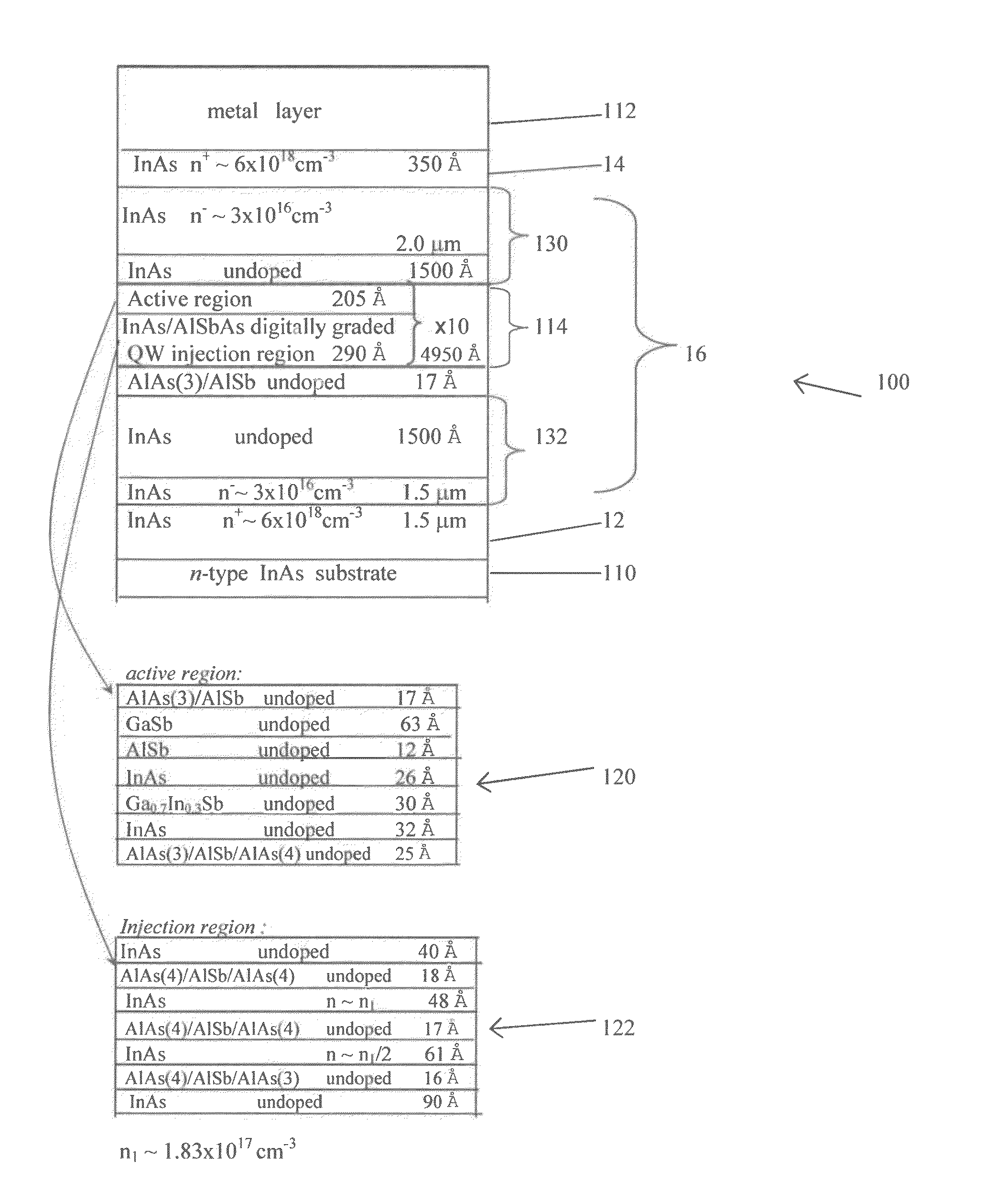
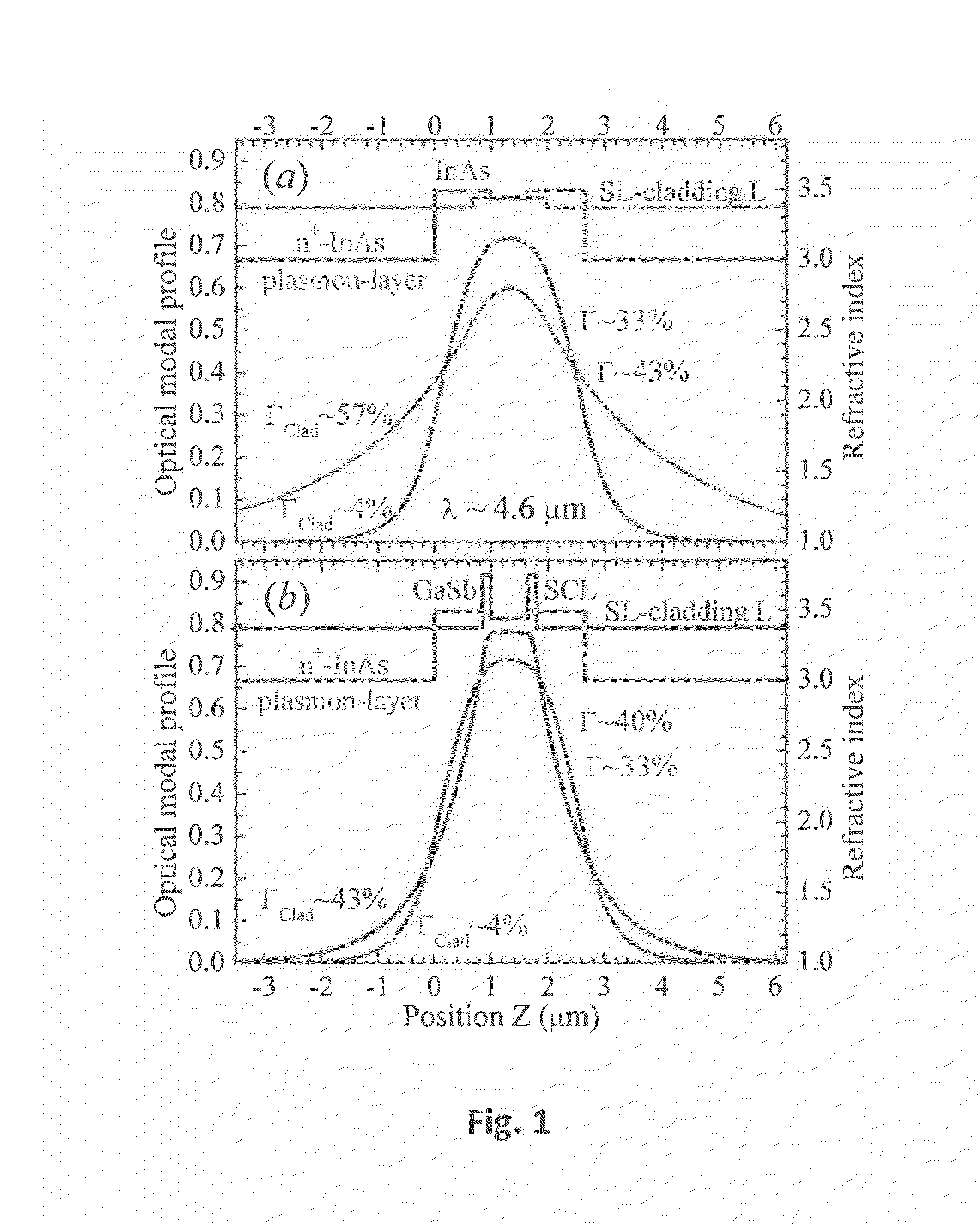
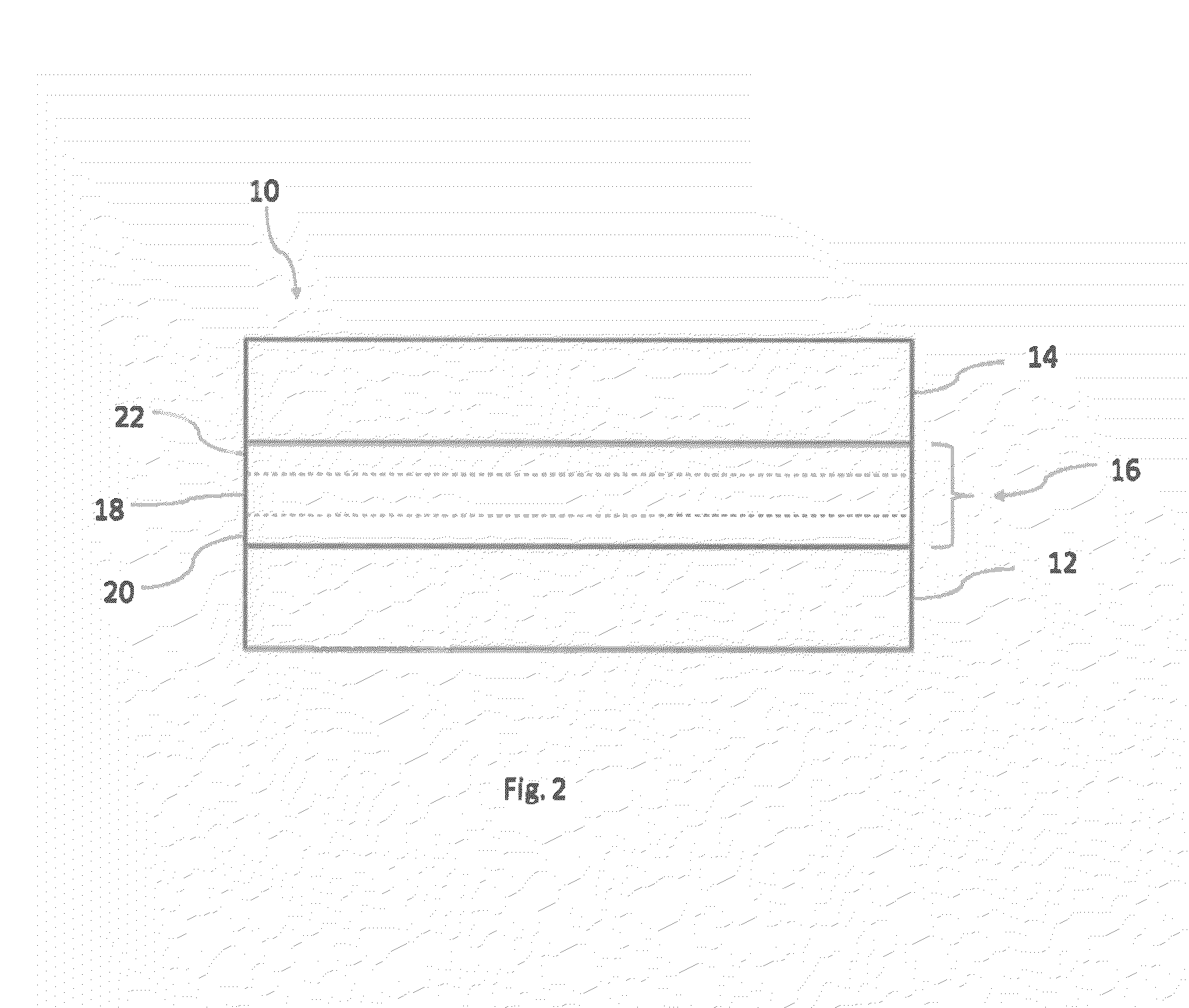
[0032]In the laser 10, the first cladding layer 12 is formed using a first high-doped semiconductor material having a first refractive index, whereas the second cladding layer 14 is formed using a second high-doped semiconductor material having a second refractive index. In this embodiment, the first and second high-doped semiconductor materials can be the same materials, or they can be formed using different materials. That is, the first high-doped semiconductor material can be a different material than the second high-doped semiconductor material. The waveguide core 16, including the active region 18, also has a waveguide core refractive index. In a preferred embodiment of the present disclosure, the first and second refractive indexes are lower than the waveguide core refractive index.

[0033]The first and second cladding layers 12 and 14 are formed with high-doped semiconductor material having doping concentrations in a range of between 1018 cm−3 to 1019 cm−3. In another aspect, t...

third embodiment

[0035]In a third embodiment, the first cladding layer 12 is formed using a first metal having a first permittivity, whereas the second cladding layer 14 is formed using a second metal having a second permittivity. Similarly, the waveguide core 16, having the active region 18, has a waveguide core permittivity. In this embodiment, the first and second permittivity is lower than the waveguide core permittivity. Exemplary metals used to form the first and / or the second cladding layers 12 and 14 include, but are not limited to, Ag, Au, Cu, Ti, Pt, Ni, and Pd, or combinations thereof.

[0036]The active region 16 is adapted to generate light based on interband transitions. As would be understood in the art, the light being generated based on interband transitions thereby defines the lasing wavelength, or the lasing frequency of the laser 10. A more particular example, of an active region 16 is described herein below with respect to the following figures. In one aspect, the active region 16 ...


PUM


Abstract

A semiconductor interband laser that includes a first cladding layer formed using a first high-doped semiconductor material having a first refractive index / permittivity and a second cladding layer formed using a second high-doped semiconductor material having a second refractive index / permittivity. The laser also includes a waveguide core having a waveguide core refractive index / permittivity, the waveguide core is positioned between the first and the second cladding layers. The waveguide core including an active region adapted to generate light based on interband transitions. The light being generated defines the lasing wavelength or the lasing frequency. The first refractive index and the second refractive index are lower than the waveguide core refractive index. The first cladding layer and / or the second cladding layers can also be formed using a metal.

Description

CROSS-REFERENCE TO RELATED APPLICATIONS[0001]This application claims benefit of U.S. Provisional Application No. 61 / 288,701, filed Dec. 21, 2009, which is incorporated herein by reference in its entirety.STATEMENT REGARDING FEDERALLY SPONSORED RESEARCH OR DEVELOPMENT[0002]This invention was made with government support under Contract Number DMR0520550 awarded by the National Science Foundation. The government has certain rights in the invention.BACKGROUND OF THE INVENTION[0003]1. Field of the Invention[0004]This invention relates to semiconductor interband lasers and more particularly, to semiconductor mid-infrared diode lasers having improved thermal dissipation and being cable of operation in longer wavelength spectrum.[0005]2. Brief Description of Related Art[0006]Semiconductor lasers have been developed with emission wavelengths (A) ranging from near- to mid-infrared (λ>3 μm) and beyond. When the wavelength of a semiconductor laser is long, the cladding layer thickness of the...

Claims


Application Information

Patent Timeline
Patent Type & Authority Patents(United States)
IPC IPC(8): H01S5/00H01S3/14B82Y20/00H01S5/10H01S5/20H01S5/22H01S5/32H01S5/34
CPCH01S5/3402B82Y20/00H01S5/1046H01S5/0014H01S5/2031H01S5/22H01S5/3216H01S5/3401H01S5/3422H01S5/3211H01S5/343
Inventor YANG, RUI Q.MISHIMA, TETSUYASANTOS, MICHAEL B.TIAN, ZHAOBINGJOHNSON, MATTHEW B.HINKEY, ROBERT T.
Owner THE BOARD OF RGT UNIV OF OKLAHOMA
Why Eureka
Try Eureka