Apparatus for and method of heat-treating thin film on surface of substrate

a technology of thin film and substrate, which is applied in the direction of heating arrangements of hot plates, lighting and heating apparatus, furniture, etc., can solve the problems of abnormal grain growth, boundary asperities, and impediments to high-precision patterning, so as to prevent abnormal grain growth

Active Publication Date: 2015-02-24
DAINIPPON SCREEN MTG CO LTD
View PDF45 Cites 14 Cited by
  • Summary
  • Abstract
  • Description
  • Claims
  • Application Information

AI Technical Summary

Benefits of technology

[0010]The flashes of light are directed onto the substrate having the surface with the thin film formed thereon to perform the baking process on the thin film. This allows the surface temperature of the thin film to rise momentarily and to fall rapidly, thereby preventing the occurrence of abnormal grain growth in the film during the baking.
[0028]It is therefore an object of the present invention to prevent abnormal grain growth in a film during baking.

Problems solved by technology

However, the process of baking a thin film by heating on a hot plate as disclosed in U.S. Patent Application Publication No. 2008 / 0008837 presents a problem such that abnormal grain growth is prone to occur in the film.
Specifically, crystal grains in the film are made coarse by heating, and the abnormal growth of some of the crystal grains results in asperities on a boundary between the thin film and an underlying substrate and on a grain boundary in some cases.
Under the circumstances of further developments for finer patterns in recent years, such asperities become an impediment to high-precision patterning.

Method used


Image

  • Apparatus for and method of heat-treating thin film on surface of substrate
  • Apparatus for and method of heat-treating thin film on surface of substrate
  • Apparatus for and method of heat-treating thin film on surface of substrate

Examples


Embodiment Construction

[0034]A preferred embodiment according to the present invention will now be described in detail with reference to the drawings.

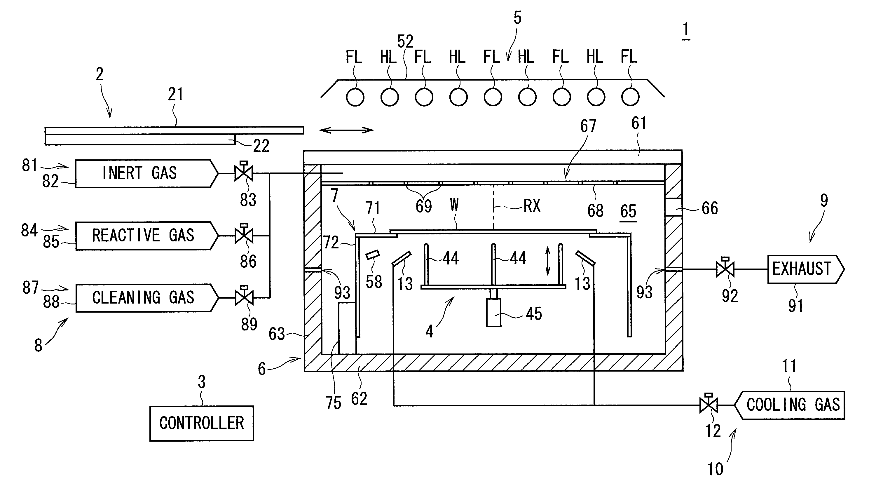
[0035]FIG. 1 is a view showing the configuration of principal parts of a heat treatment apparatus 1 according to the present invention. The heat treatment apparatus 1 is a flash lamp annealer for irradiating a substantially circular semiconductor wafer W serving as a substrate and having a front surface with a thin film formed thereon with flashes of light to perform the process of baking the thin film. In FIG. 1 and the subsequent figures, the dimensions of components and the number of components are shown in exaggeration or in simplified form, as appropriate, for the sake of easier understanding.

[0036]The heat treatment apparatus 1 principally includes a chamber 6 of a substantially cylindrical configuration for receiving a semiconductor wafer W therein, a holder 7 for holding a semiconductor wafer W within the chamber 6, a light irradiation part 5 for irr...


PUM


Abstract

A semiconductor wafer having a surface with a thin film formed thereon is transported into a chamber and held by a holder. After an atmosphere provided in the chamber is replaced, flashes of light are directed from flash lamps in a light irradiation part toward the semiconductor wafer to perform a baking process on the thin film. The irradiation of the semiconductor wafer with light from halogen lamps in the light irradiation part also starts at the same time as the irradiation thereof with the flashes of light. The flashes of light emitted for an extremely short period of time and having a high intensity allow the surface temperature of the thin film to rise momentarily. This prevents the occurrence of abnormal grain growth resulting from prolonged baking in the film.

Description

BACKGROUND OF THE INVENTION[0001]1. Field of the Invention[0002]The present invention relates to a heat treatment apparatus and a heat treatment method for performing the process of baking a thin film formed on a surface of a thin sheet-like precision electronic substrate, such as a semiconductor wafer and a glass substrate for a liquid crystal display device (hereinafter referred to simply as a “substrate”).[0003]2. Description of the Background Art[0004]Thin film formation on the substrate is an indispensable key technique for the manufacture of semiconductor devices and liquid crystal displays. For example, a resist film and an anti-reflective film are formed on a wafer in a photolithographic process for patterning on a semiconductor wafer. Also, an interlayer dielectric film for insulation and a metal film for electrode interconnection are formed on a surface of a semiconductor wafer in some cases. Further, a polycrystalline or amorphous film of silicon (Si) is formed on a glass...

Claims


Application Information

Patent Timeline
Patent Type & Authority Patents(United States)
IPC IPC(8): F27D11/00H05B7/18H05B3/68F26B3/30F27B17/00F27D7/02H01L21/67
CPCF27B17/0025F27D7/02H01L21/67109H01L21/67115
Inventor KATO, SHINICHIKIYAMA, HIROKI
Owner DAINIPPON SCREEN MTG CO LTD
Why Eureka
Try Eureka