Nano-fabricated structured diamond abrasive article

a diamond abrasive and fabricated technology, applied in the direction of gear teeth, gear-teeth manufacturing apparatus, other chemical processes, etc., can solve the problems of increasing the contact area, increasing the defect rate of the planarization process, and modifying the removal rate of the planarizing material, so as to achieve a high-controlled abrasive action and more predictable removal rate

Active Publication Date: 2015-03-17
JOHN CRANE INC
View PDF8 Cites 1 Cited by
  • Summary
  • Abstract
  • Description
  • Claims
  • Application Information

AI Technical Summary

Benefits of technology

[0010]Some methods described herein are designed to produce precision microfabricated or nanofabricated abrasive articles or polish pad conditioners. Such abrasive articles include a plurality of raised geometrical protrusions which produce abrasive action or material removal when placed into contact with a target surface with a given downward force and move in relation to the target surface. In some embodiments, the plurality of geometrical protrusions are preselected (or designed) for a specific sizes, shapes and placements on an abrasive article substrate. The geometrical protrusions are placed on the abrasive article substrate surface in tightly controlled placements and therefore it is possible to design or specify a series of protrusion placements that are highly regular to produce highly controlled abrasive action or more predictable removal rates.
[0011]In some embodiments, micro-fabricated (or nano-fabricated) conditioning disks or substrates with extremely narrow and carefully designed “grit” (i.e. geometrical protrusion) size distributions and shapes can be used. Some embodiments describe methods of fabricating such conditioners or structured abrasive articles. Such embodiments may comprise arrays of diamond tips, posts or other geometrical protrusions of well-controlled and designed geometry and distribution / placement across a disk or substrate surface. Such disks may combine the durable and monolithic nature of a diamond abrasive surface which impedes the loss of grit “particles” (abrasive structures or geometrical protrusions made of or coated with diamond), with ultra-narrow height distribution or controlled size distribution and placement of grit particles / geometrical protrusions. The geometry and surface density of the diamond spikes / geometrical protrusions can also be very well controlled and optimized, with negligible variation from conditioning disk to conditioning disk or from precision abrasive surface to precision abrasive surface.

Problems solved by technology

During the CMP process, the surface of the polishing pad may be gradually saturated with polishing nanoparticles, polishing debris and portions of abraded pad material, thus potentially increasing the contact area to an extent that modifies the removal rate of the planarizing material and / or increases the rate of defects of the planarization process through scratching of various sizes.
In addition, the polishing pad surface can be abraded leading to a less controlled polishing process of the substrate being removed.
Metal embedded diamond grit particles can also loosen and fall off, generating scratches or other defects on the substrates that are being planarized.
However, for a range of applications, such as damascene and double damascene technologies, and as feature dimensions for silicon process technology continue to shrink in the sub-100 nm range, even such improved conditioning technology may still be prone to limitations imposed by irreproducibility in CMP removal rates and pad lifetime.
Another issue with these embedded grit pads is that during the wear process of the conditioners, some of the embedded diamond particles may break or be dislodged.
Since they might be quite large (e.g. 10-50 μm) hard diamond particles, they can be a significant source of defects on wafers as they are known to cause large scratches on polishing surfaces which can cause failure or reliability problems with surfaces polished by the pads being conditioned.

Method used


Image

  • Nano-fabricated structured diamond abrasive article
  • Nano-fabricated structured diamond abrasive article
  • Nano-fabricated structured diamond abrasive article

Examples


first embodiment

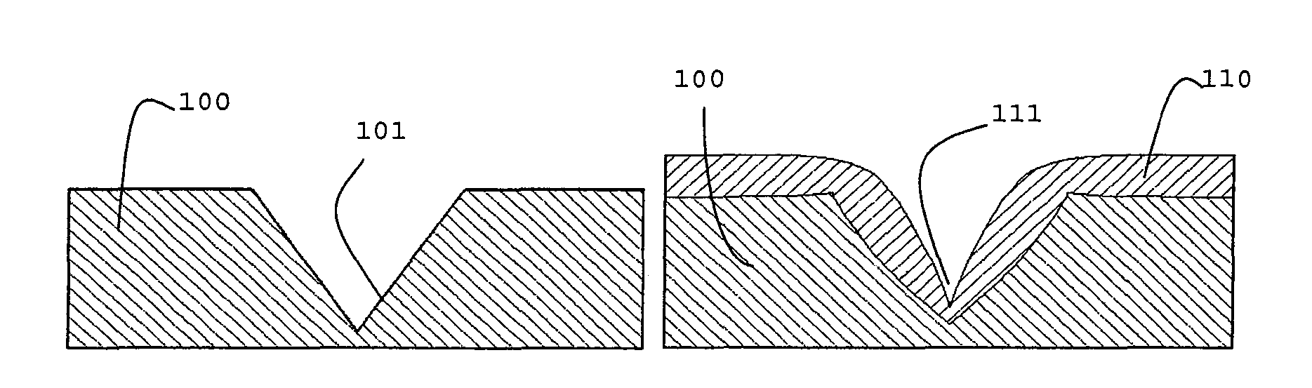
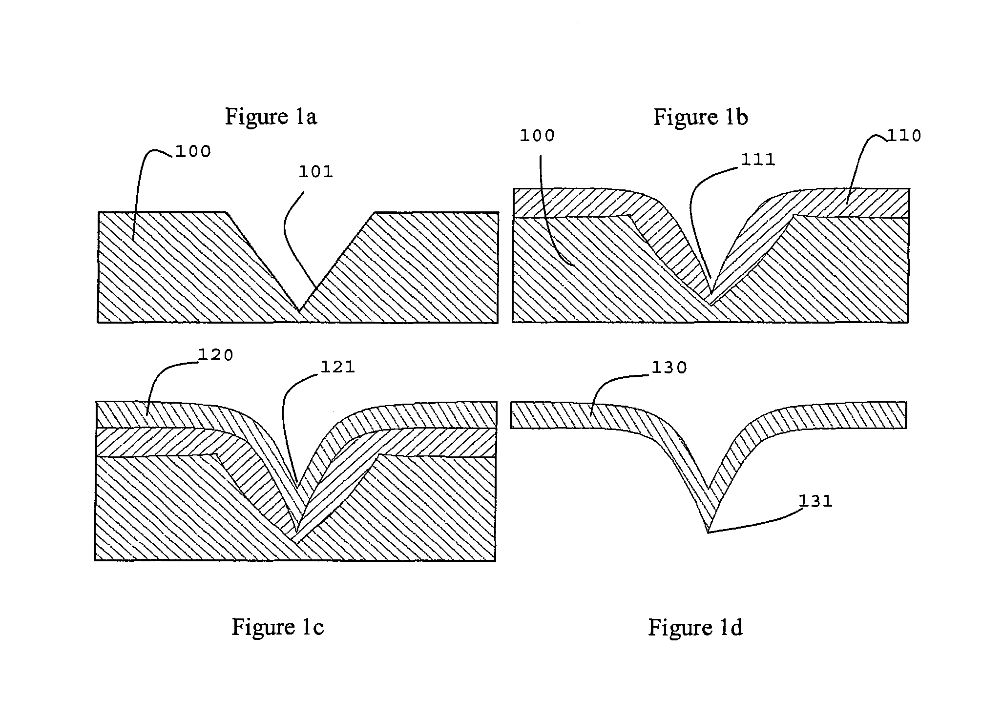
[0027]A first embodiment comprises starting with a Si wafer substrate, followed by SiO2 growth (e.g. ˜0.3 μm) by thermal oxidation, followed by lithographic patterning and crystallographic wet etching of the exposed substrate surface with square or circular windows of size ˜2 to 30 μm (and preferably of size 5-20 μm, e.g. 14 μm), in regularly-spaced patterns or assembly to produce a desired density of spikes / geometrical protrusions (e.g. ˜300,000 / cm2). However, any desired pattern can be designed into the lithographic step to produce an essentially unlimited range of possible arrangements and designed structure placements, sizes and shapes. The SiO2 is then removed by buffered HF or oxide CMP. Optionally, a seeding enhancement layer (such as 50 nm of sputtered W) can be deposited before diamond deposition. Seeding with a suspension of diamond nanoparticles (prepared, e.g., by ultrasonication and rinsing, with detonation diamond powder dissolved in methanol, or with ultra-dispersed d...

second embodiment

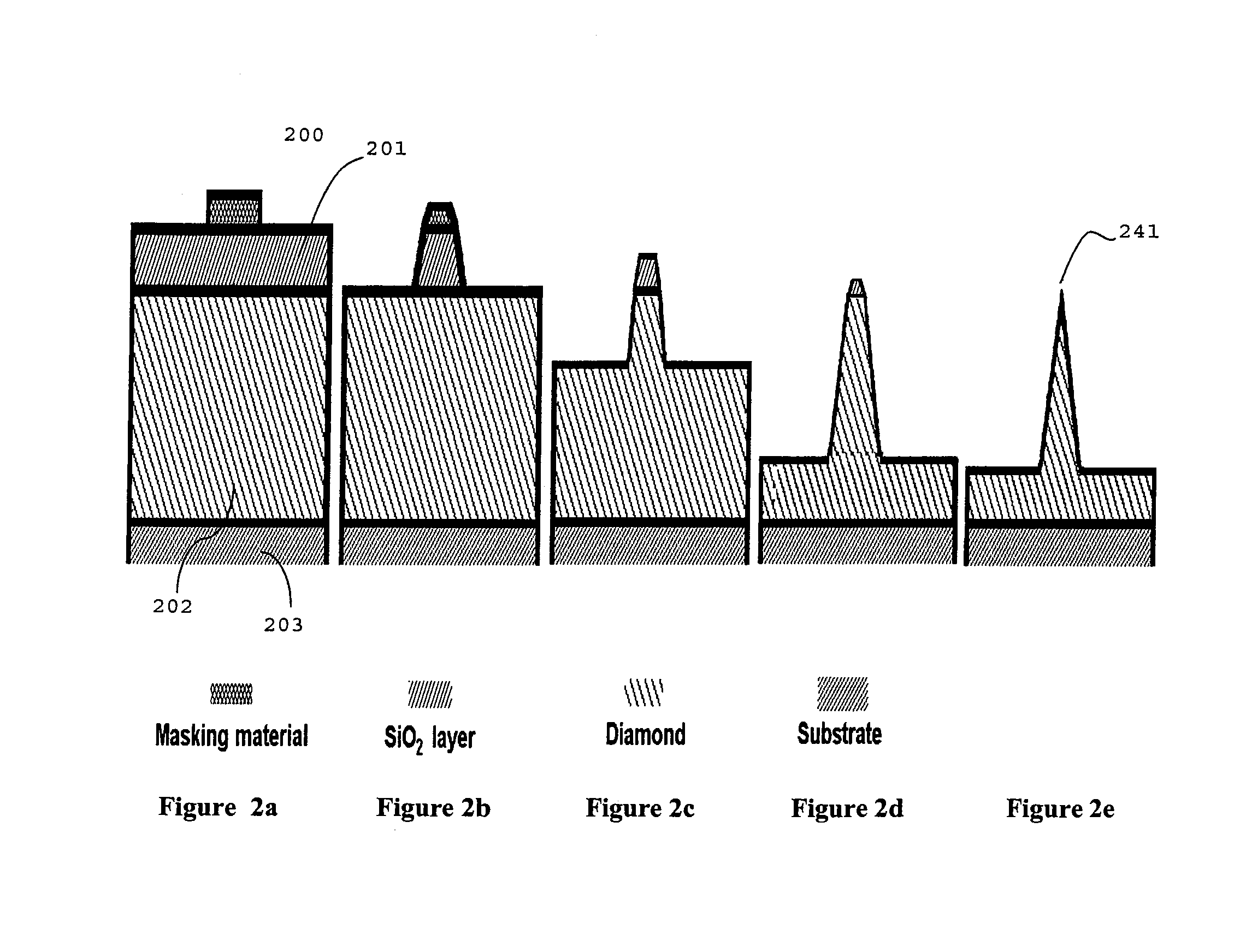
[0030]A second embodiment comprises direct etching (or forming) of spikes / geometrical protrusions into a thick diamond layer, for example from a thick UNCD layer (e.g. ˜15 μm) deposited by HFCVD onto a planar ceramic or silicon substrate. This is followed by: a piranha clean of the UNCD layer (which also has as a goal to modify the hydrogen termination on the diamond surface into an oxide (—O) or a hydroxyl (—OH) termination which can provide for enhanced adhesion with a metallic or hydrophylic materials; deposition by PECVD of a SiO2 layer (e.g. ˜1.5 μm); CMP planarization (e.g. with a Cabot Microelectronics SS12 slurry and a Rohm and Haas, IC 1000 polishing pad, under 20 psi downward force polishing pressure) by removing ˜1 μm of the SiO2, to leave behind a smooth, planar surface of SiO2, acceptable for lithography. This film is then patterned lithographically and etched (e.g. with CHF3—O2 reactive ion etching) into an array of square islands, (e.g. ˜4 μm in size), then the patter...

third embodiment

[0032]A third embodiment comprises preparing an etched or fabricated of Si or other patternable substrate to form spikes / geometrical protrusions that may then be covered with a diamond film or layer. For example, a Si wafer may be covered with a layer of thermal oxide, e.g. ˜0.5 μm in thickness, or a layer of CVD oxide or nitride or other materials that are resistant to an etch chemistry used to etch silicon. The oxide (or alternative material resistant to silicon etch) may then be patterned into an array of square (or other desired shape) islands, each of them being e.g. ˜6 μm×6 μm in size, by wet etching, with a buffered HF etch, NH4F:HF 1:6, through a photoresist mask. The Si may then be etched with a SF6 / O2 plasma Reactive Ion Etch (RIE) (e.g. 50 sccm SF6, 5 sccm O2, 200 mTorr, 200W) having a slightly isotropic etching nature. The degree of anisotropy may vary from one piece of equipment to another, and depends upon, for example, the plate area and the surface area being etched....


PUM

PropertyMeasurementUnit
grain sizeaaaaaaaaaa
heightaaaaaaaaaa
heightaaaaaaaaaa

Abstract

The present invention describes a microfabricated or nanofabricated structured diamond abrasive with a high surface density array of geometrical protrusions of pyramidal, truncated pyramidal or other shape, of designed shapes, sizes and placements, which provides for improved conditioning of CMP polishing pads, or other abrasive roles. Three methods of fabricating the structured diamond abrasive are described: molding of diamond into an array of grooves of various shapes and sizes etched into Si or another substrate material, with subsequent transferal onto another substrate and removal of the Si; etching of an array of geometrical protrusions into a thick diamond layer, and depositing a thick diamond layer over a substrate pre-patterned (or pre-structured) with an array of geometrical protrusions of designed sizes, shapes and placements on the surface.

Description

CROSS-REFERENCE TO RELATED APPLICATIONS[0001]This application claims priority from U.S. Provisional Patent application Ser. No. 61 / 060,717 entitled “Nanofabricated Structured Diamond Abrasive Article”, filed Jun. 11, 2008, which is incorporated herein by reference in its entirety.TECHNICAL FIELD[0002]Some embodiments are related to methods and an article for abrasion or conditioning of polishing pads and more particularly to methods of manufacture of precision microfabricated or nanofabricated diamond abrasive surfaces with designed placement of geometrical protrusions capable of generating abrasion of designed shape and size.BACKGROUND OF THE INVENTION[0003]Chemical Mechanical Polishing or Planarization (CMP) is a planarization method used in the semiconductor industry and in other industries such as the optical and flat panel polishing industries, which typically involves removal of material by a combination of relatively gentle abrasion of the layer being planarized (e.g. a Si wa...

Claims


Application Information

Patent Timeline
Patent Type & Authority Patents(United States)
IPC IPC(8): B24D18/00B24D3/06
CPCB24D3/06B24D18/00Y10T428/24612
Inventor MOLDOVAN, NICOLAIECARLISLE, JOHN
Owner JOHN CRANE INC
Why Eureka
Try Eureka