Nano-fabricated Structured Diamond Abrasive Article
a diamond abrasive and fabricated technology, applied in the direction of gear teeth, gear-teeth manufacturing apparatus, other chemical processes, etc., can solve the problems of increasing the contact area, increasing the defect rate of the planarization process, and modifying the removal rate of the planarizing material, so as to achieve a high-controlled abrasive action and more predictable removal rate
- Summary
- Abstract
- Description
- Claims
- Application Information
AI Technical Summary
Benefits of technology
Problems solved by technology
Method used
Image
Examples
first embodiment
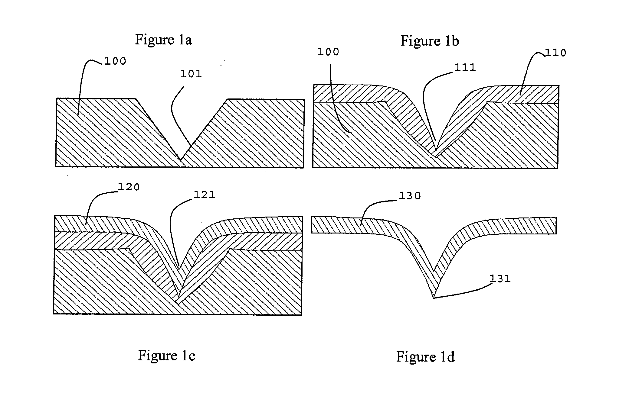
[0027]A first embodiment comprises starting with a Si wafer substrate, followed by SiO2 growth (e.g. ˜0.3 μm) by thermal oxidation, followed by lithographic patterning and crystallographic wet etching of the exposed substrate surface with square or circular windows of size ˜2 to 30 μm (and preferably of size 5-20 μm, e.g. 14 μm), in regularly-spaced patterns or assembly to produce a desired density of spikes / geometrical protrusions (e.g. ˜300,000 / cm2). However, any desired pattern can be designed into the lithographic step to produce an essentially unlimited range of possible arrangements and designed structure placements, sizes and shapes. The SiO2 is then removed by buffered HF or oxide CMP. Optionally, a seeding enhancement layer (such as 50 nm of sputtered W) can be deposited before diamond deposition. Seeding with a suspension of diamond nanoparticles (prepared, e.g., by ultrasonication and rinsing, with detonation diamond powder dissolved in methanol, or with ultra-dispersed d...
second embodiment
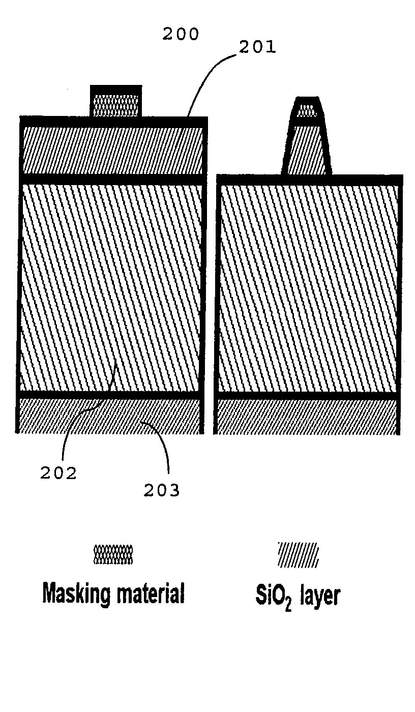
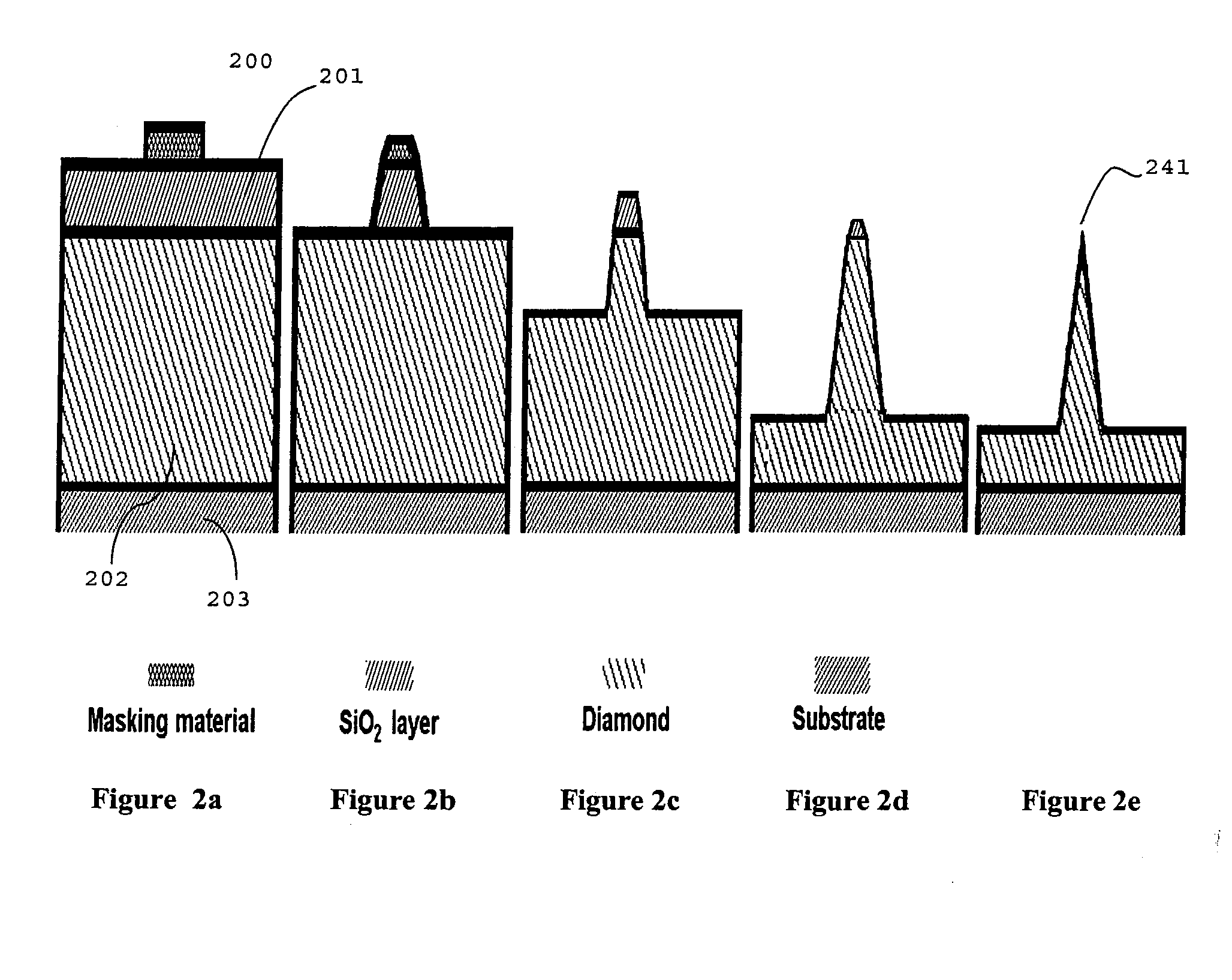
[0030]A second embodiment comprises direct etching (or forming) of spikes / geometrical protrusions into a thick diamond layer, for example from a thick UNCD layer (e.g. ˜15 μm) deposited by HFCVD onto a planar ceramic or silicon substrate. This is followed by: a piranha clean of the UNCD layer (which also has as a goal to modify the hydrogen termination on the diamond surface into an oxide (—O) or a hydroxyl (—OH) termination which can provide for enhanced adhesion with a metallic or hydrophylic materials; deposition by PECVD of a SiO2 layer (e.g. ˜1.5 μm); CMP planarization (e.g. with a Cabot Microelectronics SS12 slurry and a Rohm and Haas, IC 1000 polishing pad, under 20 psi downward force polishing pressure) by removing ˜1 μm of the SiO2, to leave behind a smooth, planar surface of SiO2, acceptable for lithography. This film is then patterned lithographically and etched (e.g. with CHF3—O2 reactive ion etching) into an array of square islands, (e.g. ˜4 μm in size), then the patter...
third embodiment
[0032]A third embodiment comprises preparing an etched or fabricated of Si or other patternable substrate to form spikes / geometrical protrusions that may then be covered with a diamond film or layer. For example, a Si wafer may be covered with a layer of thermal oxide, e.g. ˜0.5 μm in thickness, or a layer of CVD oxide or nitride or other materials that are resistant to an etch chemistry used to etch silicon. The oxide (or alternative material resistant to silicon etch) may then be patterned into an array of square (or other desired shape) islands, each of them being e.g. ˜6 μm×6 μm in size, by wet etching, with a buffered HF etch, NH4F:HF 1:6, through a photoresist mask. The Si may then be etched with a SF6 / O2 plasma Reactive Ion Etch (RIE) (e.g. 50 sccm SF6, 5 sccm O2, 200 mTorr, 200W) having a slightly isotropic etching nature. The degree of anisotropy may vary from one piece of equipment to another, and depends upon, for example, the plate area and the surface area being etched....
PUM
| Property | Measurement | Unit |
|---|---|---|
| Grain size | aaaaa | aaaaa |
| Time | aaaaa | aaaaa |
| Length | aaaaa | aaaaa |
Abstract
Description
Claims
Application Information


