Method for producing optical semiconductor device

a semiconductor and optical technology, applied in semiconductor/solid-state device testing/measurement, instruments, other domestic articles, etc., can solve the problem of difficult to form a resin layer on the wafer with a uniform thickness, and achieve the effect of improving the uniform thickness distribution of resin, reducing the opening, and adjusting more accurately

Active Publication Date: 2015-03-24
SUMITOMO ELECTRIC IND LTD
View PDF2 Cites 4 Cited by
  • Summary
  • Abstract
  • Description
  • Claims
  • Application Information

AI Technical Summary

Benefits of technology

[0009]The second arrangement structure includes a plurality of mesas defined by trenches having different trench widths from each other. According to considering a variation of the thickness of the resin layer formed on the second arrangement structure, the thickness of the resin layer varies depending on the difference in the trench width of the trench structure. Using the difference in the thickness distribution of the resin layer between the first arrangement structure and the second arrangement structure, the thickness of the resin layer can be adjusted by controlling the trench structure serving as a base on which the resin layer is to be formed. Specifically, the trench width of the trench structure is determined in each of the sections in the section arrangement of a semiconductor device using the in-plane distribution of the thickness of the resin layer formed on the first arrangement structure and the correlation between the trench width and the thickness of the resin layer formed on the second arrangement structure. Thus, a trench width map on the wafer is formed. A mask including a pattern of the semiconductor mesa and the trench having the trench width based on the trench width map is formed. A stacked semiconductor layer formed on a substrate is etched using the mask to form a trench structure including the semiconductor mesa and the trench that defines the semiconductor mesa. Thus, the trench width of the trench that defines the semiconductor mesa is changed in a plurality of sections in each of which the semiconductor device is formed. Subsequently, a resin layer is formed on the trench structure, whereby the thickness of the resin layer is adjusted in accordance with the pattern of the trench width based on the trench width map. As a result, the thickness of the resin layer is made substantially uniform in the wafer plane. When an opening is formed on the semiconductor mesa by etching the resin layer, the variation of the opening can be reduced.
[0010]The production method according to an embodiment of the present invention may further include a step of obtaining an in-plane distribution of the etching rate by measuring an etching rate of a resin layer formed on a wafer having the wafer size. In the step of forming the trench width map, the trench width of the trench in the optical semiconductor device may be determined using the in-plane distribution of the thickness, the in-plane distribution of the etching rate, and the correlation between the thickness of the resin layer and the trench width. The in-plane distribution of the etching rate in the wafer plane is independent of the thickness distribution of the resin layer. In the formation of the trench width map, the trench width of the trench in the optical semiconductor device is determined in consideration of the in-plane distribution of the etching rate in the wafer plane in addition to the in-plane distribution of the thickness of the resin and the correlation between the thickness of the resin layer and the trench width. Thus, the thickness of the resin layer formed on the trench structure can be adjusted more accurately, which can improve the uniformity of the thickness distribution of the resin. As a result, the variation of the opening can be further reduced.
[0014]According to this production method, the adjustment of the trench width is performed on the interval between the semiconductor terrace and the semiconductor mesa. In addition, in the arrangement of sections for optical semiconductor devices arranged in the wafer plane, the trench width in one of the sections is different from the trench width in another one of the sections. This difference in the trench width can ensure high uniformity between the opening in one of the sections and the opening in another one of the sections.
[0019]According to this production method, the trench is filled with the resin. The thermal expansion coefficient of the resin is different from that of a semiconductor. Therefore, when the trench width is increased in the wafer plane, the resin layer is detached due to the difference in thermal expansion coefficient. However, by forming the dummy semiconductor mesa in the trench, the trench is constituted by a plurality of sub-trenches and the volume of the resin layer in each trench can be decreased without affecting the resin thickness adjusted in accordance with the trench width so much. This can suppress the detachment of the resin layer caused by the difference in thermal expansion coefficient.

Problems solved by technology

Herein, it is difficult to form a resin layer on the wafer with a uniform thickness.

Method used


Image

  • Method for producing optical semiconductor device
  • Method for producing optical semiconductor device
  • Method for producing optical semiconductor device

Examples


example

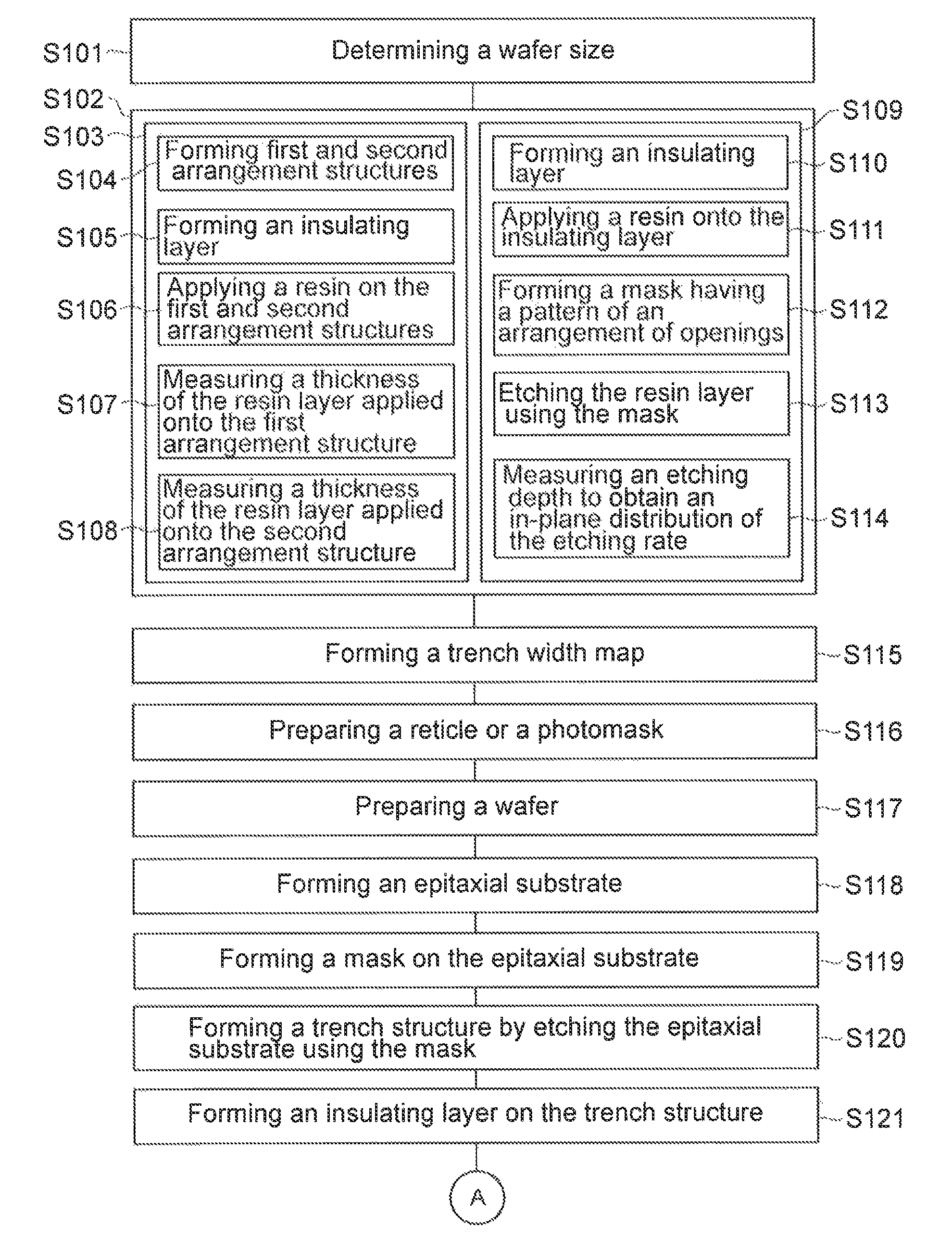
[0093]A method for designing a mask whose trench width is corrected to make the opening shape of a BCB resin layer uniform in a wafer plane will be described. In this Example, the exposure that uses a stepper will be described. The description can also be applied to the exposure that uses a mask aligner.

[0094]To obtain the relationship between the trench width and the thickness of the BCB resin layer on a semiconductor mesa, the height of the semiconductor mesa, the width of the semiconductor mesa, and the thickness of the BCB resin layer on the semiconductor mesa are determined. One example is shown below.[0095]Height of semiconductor mesa: 3 μm[0096]Depth of isolation mesa: 0.8 μm[0097]Width of semiconductor mesa: 1.5 μm[0098]Thickness of BCB resin layer on semiconductor mesa: 3 μm

The used reticle has two types of patterns. A single reticle has a pattern in which the trench width beside the semiconductor mesa is fixed to measure the thickness distribution of the BCB resin layer in...


PUM

PropertyMeasurementUnit
widthaaaaaaaaaa
heightaaaaaaaaaa
thicknessaaaaaaaaaa

Abstract

A method for producing an optical semiconductor device includes the steps of determining a wafer size to make a section arrangement including a plurality of sections in each of which the optical semiconductor device including a semiconductor mesa is formed; obtaining an in-plane distribution of a thickness of a resin layer on a wafer; obtaining a correlation between a thickness of a resin layer and a trench width; forming a trench width map using the in-plane distribution of the thickness and the correlation; preparing an epitaxial substrate by forming a stacked semiconductor layer; forming, on the epitaxial substrate, a mask based on the trench width map; forming a trench structure including the semiconductor mesa by etching the stacked semiconductor layer using the mask; forming a resin layer on the trench structure; and forming an opening on the semiconductor mesa by etching the resin layer.

Description

BACKGROUND OF THE INVENTION[0001]1. Field of the Invention[0002]The present invention relates to a method for producing an optical semiconductor device.[0003]2. Description of the Related Art[0004]Non-Patent Document 1 (K. Tsuzuki, T. Ishibashi, T. Ito, S. Oku, Y. Shibata, R. Iga, Y. Kondo and Y. Tohmori, 40 Gbit / s n / i / n InP Mach-Zehnder modulator with a π voltage of 2.2 V, Electronics Letters Online 2nd, Oct. 2003, Vol. 39 No. 20) describes a Mach-Zehnder modulator. The Mach-Zehnder modulator includes a high-mesa-shaped semiconductor layer disposed on a semiconductor substrate. The high-mesa-shaped semiconductor layer is buried with a protective layer. Thus, the semiconductor layer has a side surface on which the protective layer is disposed.SUMMARY OF THE INVENTION[0005]Semiconductor Mach-Zehnder modulators are constituted by two optical waveguides and two optical couplers for optically coupling the optical waveguides. In general, an optical waveguide is constituted by a semicondu...

Claims


Application Information

Patent Timeline
Patent Type & Authority Patents(United States)
IPC IPC(8): B29D11/00G02F1/025G02F1/225
CPCG02F1/2257G02F1/025G02B6/136G02B2006/121G02B2006/12173G06F30/39G02F1/212H01L21/31116H01L22/12H01L22/20H01L33/44
Inventor KITAMURA, TAKAMITSUYAGI, HIDEKI
Owner SUMITOMO ELECTRIC IND LTD
Why Eureka
Try Eureka