Radiation-hardened memory storage unit

a technology of memory storage unit and hardened memory, which is applied in the direction of information storage, static storage, digital storage, etc., can solve the problems of substantial increase in storage unit area and memory is one of the most vulnerable parts, and achieve the effect of simple circui

Inactive Publication Date: 2015-03-31
HUAZHONG UNIV OF SCI & TECH
View PDF8 Cites 26 Cited by
  • Summary
  • Abstract
  • Description
  • Claims
  • Application Information

AI Technical Summary

Benefits of technology

[0025]Advantages of the invention are as follows. Firstly, total ionizing dose radiation hardening can be realized automatically in a small storage unit area. As the memory storage unit of the invention is formed by PMOS transistors and the majority carrier in the substrate of a PMOS transistor is the electron, the leakage current channel cannot be formed between the drain and the source of a PMOS transistor by the total ionizing dose radiation and no leakage current exists, and therefore, the total ionizing dose radiation hardening is not necessary for a PMOS transistor. Secondly, the circuit is simple and can be realized directly by commercial CMOS processes without any changes to the existing processes.

Problems solved by technology

Therefore, the memory is one of the most vulnerable parts in an aerospace electronic system for its high density.
However, methods for hardening total ionizing dose radiation in FIG. 2 and FIG. 3 may result in a substantial increase in storage unit area.

Method used


Image

  • Radiation-hardened memory storage unit
  • Radiation-hardened memory storage unit
  • Radiation-hardened memory storage unit

Examples


Embodiment Construction

[0032]To further illustrate the invention, experiments detailing a radiation-hardened memory storage unit that is resistant to total ionizing dose effects are described below. It should be noted that the following examples are intended to describe and not to limit the invention.

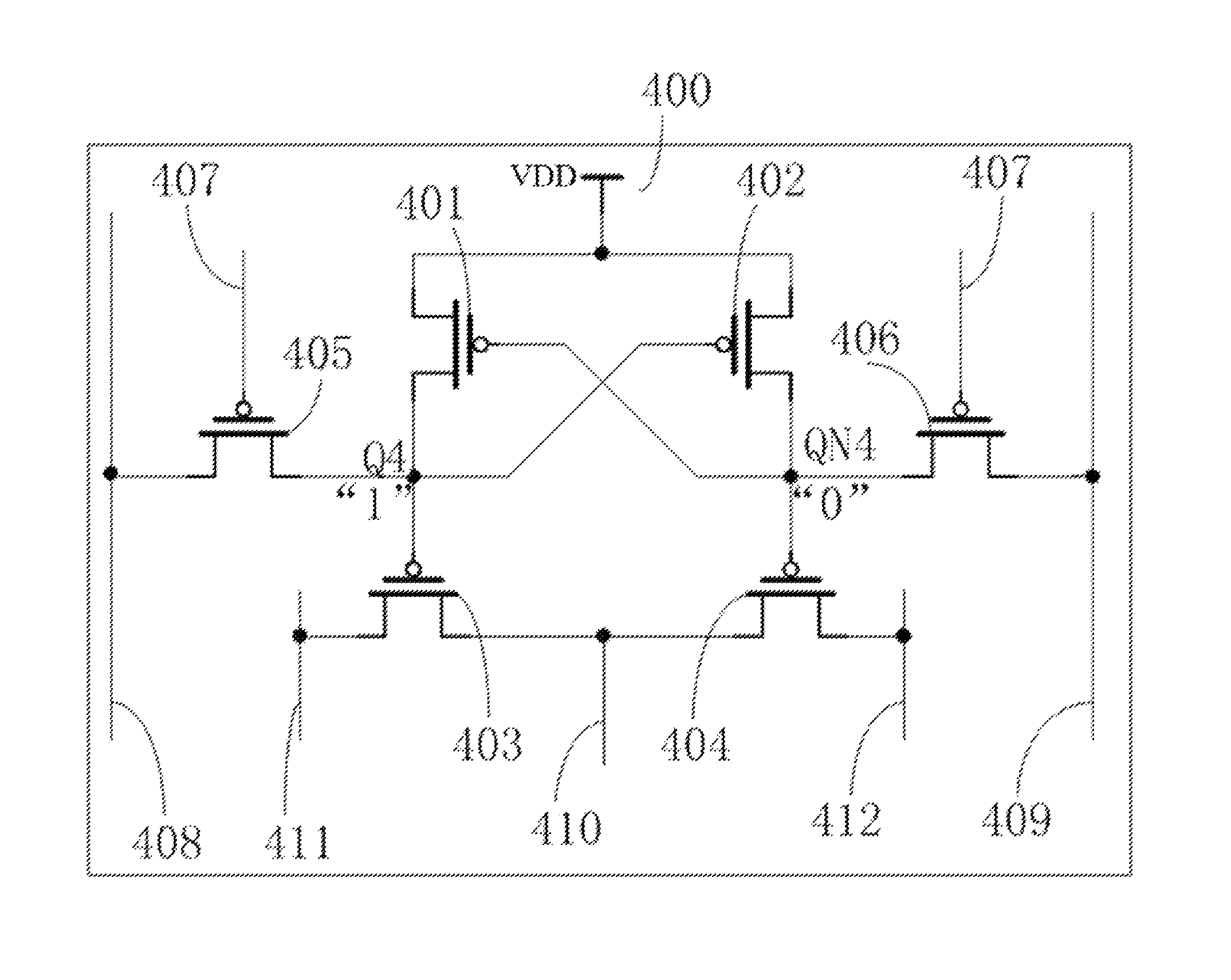
[0033]FIG. 4 is a schematic diagram of a radiation-hardened memory storage unit that is resistant to total ionizing dose effects according to one embodiment of the present invention. As in FIG. 4, a storage unit 400 comprises six PMOS transistors 401-406, and the substrates of all the six PMOS transistors are coupled to a voltage VDD.

[0034]A first PMOS transistor 401 and a second PMOS transistor 402 are pull-up transistors. A source of the first PMOS transistor 401 is coupled to a voltage VDD, a gate of the first PMOS transistor 401 is coupled to a reverse storage node QN4, and a drain of the first PMOS transistor 401 is coupled to a storage node Q4. A source of the second PMOS transistor 402 is coupled to th...


PUM


Abstract

A radiation-hardened memory storage unit that is resistant to total ionizing done effects, the unit including PMOS transistors.

Description

CROSS-REFERENCE TO RELATED APPLICATIONS[0001]Pursuant to 35 U.S.C. §119 and the Paris Convention Treaty, this application claims the benefit of Chinese Patent Application No. 201310398912.4 filed Sep. 4, 2013, the contents of which are incorporated herein by reference. Inquiries from the public to applicants or assignees concerning this document or the related applications should be directed to: Matthias Scholl P.C., Attn.: Dr. Matthias Scholl Esq., 14781 Memorial Drive, Suite 1319, Houston, Tex. 77079.BACKGROUND OF THE INVENTION[0002]1. Field of the Invention[0003]The invention relates to a radiation-hardened memory storage unit that is resistant to total ionizing dose effects.[0004]2. Description of the Related Art[0005]In aerospace electronic systems, the memory is a very important part occupying most of the chip area. In the space environment, an electronic system suffers radiations from the Galaxy, the Sun, the Earth and other radiators. Therefore, the memory is one of the most...

Claims


Application Information

Patent Timeline
Patent Type & Authority Patents(United States)
IPC IPC(8): G11C5/06
CPCG11C5/063G11C11/4125
Inventor SANG, HONGSHIWANG, WENZHANG, TIANXULIANG, CHAOBINGZHANG, JINGXIE, YANGYUAN, YAJING
Owner HUAZHONG UNIV OF SCI & TECH
Why Eureka
Try Eureka