Metamaterials with terahertz response and methods of making same

a technology of terahertz response and metals, applied in the field of metals, can solve the problems of limited thz device scope, difficult to find natural materials with the necessary properties, and inability to fabricate mtms into bulk three-dimensional slabs

Inactive Publication Date: 2015-05-12
NEW JERSEY INSTITUTE OF TECHNOLOGY
View PDF6 Cites 9 Cited by
  • Summary
  • Abstract
  • Description
  • Claims
  • Application Information

AI Technical Summary

Benefits of technology

[0008]Embodiments of the present disclosure provide metamaterial (MTM) structures in the THz range. MTMs in accordance with the present disclosure enable an artificial magnetic component for the implementation of devices at THz frequencies such as THz sources, harmonics generators, photo mixers and the like. Metamaterials made in accordance with the present disclosure also make possible the development of novel devices for biological and security sensing and are used as antenna radomes or as a frequency selective surface to control the direct emission of radiation sources.
[0011]In accordance with another embodiment, a novel method of fabrication of MTMs is disclosed employing a microfluidic-jetted technique for making two- and three-dimensional conventional MTMs in the terahertz region. Using this novel method, for the first time MTMs can be fabricated on a flexible substrate, thus adding the potential for future market applications. In addition, using the microfluidic-jetted technique, miniature three-dimensional THz MTMs can be achieved by stacking the two-dimensional structures in layers. Microfluidic-jetting is a variation of ink-jet printing techniques and is currently being evaluated as a precision deposition tool in a variety of manufacturing processes such as Liquid Crystal Display (LCD) and Organic Light Emitter Diode (OLED). See, W. Wong, Inkjet printer draws the line in manufacturing technology, Electronic Design, 53 (25), 25, (2005); J. C. Sturm, et al., Printing approaches for large-area color organic LED displays, Proc. of SPIE—The International Society for Optical Engineering, 3797, 266-274, (1999); S. C. Chang, et al., “Multicolor organic light-emitting diodes processed by hybrid inkjet printing,”Adv. Materials, 11 (9), 734-737, (1999). The methods disclosed herein provide economic advantages in cases in which the deposited material is expensive. By eliminating the use of die or photomask the presently disclosed methods reduce fabrication cost and minimize fabrication time, resulting in the ability to prototype rapidly. In addition, the microfludic-jetted technique offers the advantage of non-contact, thus minimizing risk of contamination. The methods can be used in conjunction with any suitable substrate and can be used to deposit a wide variety of material, thereby providing great design flexibility. The nozzle sizes of the microfluidic jet can be varied depending on the application and the desired design.

Problems solved by technology

It is difficult to find a natural material which has the necessary properties or material parameters required for certain applications.
Certain ferromagnetic and antiferromagnetic materials such as InGaMnAs / InP and GdMnO3 exhibit a very weak magnetic response over a frequency range of several hundred gigahertz which limit the scope of possible THz devices.
Nearly all of the MTMs that exist in the terahertz region are single, two-dimensional layers fabricated on a rigid substrate due to the limitation of the conventional MEMs technique.
This is mainly due to the inability in fabricating the MTMs into a bulk three-dimensional slab.

Method used


Image

  • Metamaterials with terahertz response and methods of making same
  • Metamaterials with terahertz response and methods of making same
  • Metamaterials with terahertz response and methods of making same

Examples


example 1

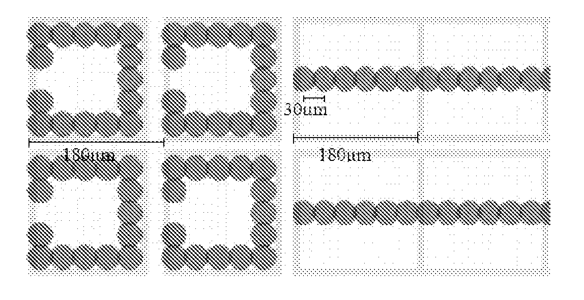
[0048]Now referring to FIG. 1, patterns of split ring resonator (SRR) and microstrips structures were deposited on top of a copper-clad Kapton® polyimide sheet with liquid polyimide using a microfluidic-jetted technique by microdroplet generation of approximately 1 pL. The liquid polyimide was purchased from HD MicroSystem® and mixed with a solvent, Pyralin thinner, in a ratio of 1:8 parts. This fluid is supplied as a solution suitable for the coating application. It can be coated onto a variety of metals and is inert with respect to the etchant, thus it is suitable to use as masking material for fabrication of copper samples. The microdroplets were placed drop by drop on the substrate to form the final desired pattern. The patterned copper clad Kapton sheet was then subjected to an etching process before it was annealed at 160° C. for 30 minutes. The deposited polyimide patterns act as a mask to prevent the copper under the pattern from being etched away by the etchant.

[0049]Table ...

example 2

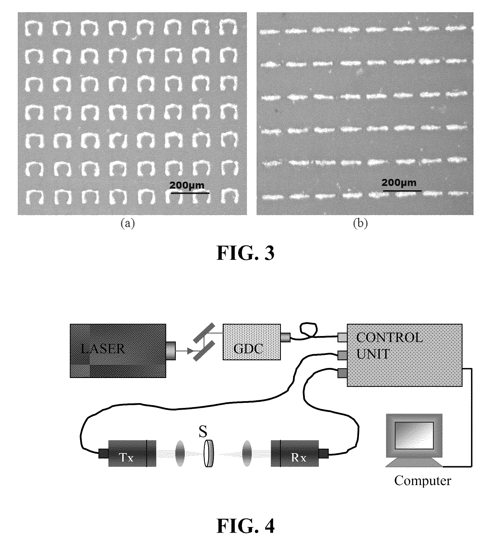
[0073]Three-dimensional alternative-stacking nanogold Left-handed metamaterials with structure lattice size of 200 micron were designed and evaluated using a THz spectroscopy system. The fabrication steps for the metamaterials are elaborated as follows.

[0074]Now referring to FIG. 11, a SRR (p=180 μm) was deposited on Kodak EasyShare matte photopaper. The deposited material was dodecanethiol functionalized nanogold having 4-5 nm particle size in 2% in toluene having ˜10 cps viscosity. The drop size was ˜30 μm using a 1 pL cartridge. Thickness of the structures was 38.7 nm. The image was taken by a built in Fiducial camera.

[0075]Now referring to FIG. 12, a SRR (p=80 μm) was deposited on a 127 μm thick polyimide substrate. The deposited material was a conductive polymer PEDT / PSS with ˜11 cps viscosity. The drop size was ˜18 μm using a 1 pL cartridge. The thickness of the structure was 0.7 μm. The image magnification is 20× using a bright field microscope.

[0076]Now referring to FIG. 13,...


PUM

PropertyMeasurementUnit
lattice sizeaaaaaaaaaa
frequenciesaaaaaaaaaa
resonance frequenciesaaaaaaaaaa

Abstract

Flexible metamaterials and three-dimensional metamaterials operable in the terahertz range are disclosed. Methods are disclosed for fabricating terahertz response metamaterials using microfluidic-jetted techniques. Layers of material including substrate and deposited material are stacked to form three dimensional bulk metamaterials. The fabricated metamaterials act as left-handed metamaterials in the range 0.1 to 3.0 THz.

Description

CROSS-REFERENCE TO RELATED APPLICATIONS[0001]This application claims the benefit of U.S. Provisional Patent Application No. 61 / 167,745 filed Apr. 8, 2009, the entirety of which is incorporated herein by reference.FIELD OF THE INVENTION[0002]This invention relates to metamaterials and in particular, to metamaterials having a terahertz response and methods of making same.BACKGROUND OF THE INVENTION[0003]Natural materials have some restrictions on their electromagnetic properties. It is difficult to find a natural material which has the necessary properties or material parameters required for certain applications. This problem usually can be solved by using metamaterials.[0004]Metamaterials (hereinafter referred to as MTMs) are defined as artificial materials which achieve extraordinary electromagnetic properties that are not possible in natural material. Although composite materials have been investigated for many years, MTMs really form a new field of science and engineering. If one ...

Claims


Application Information

Patent Timeline
Patent Type & Authority Patents(United States)
IPC IPC(8): H01F27/30G01N21/3581G02B1/00H01P1/203H01P7/08H01Q15/00
CPCG02B1/007H01P1/20381H01P7/082H01Q15/0026H01Q15/0086G01N21/3581
Inventor HOR, YEW LILIM, HEE CHUANHOR, YEW FONGFEDERICI, JOHN FRANCIS
Owner NEW JERSEY INSTITUTE OF TECHNOLOGY
Why Eureka
Try Eureka