Electron-multiplication image sensor

a multi-segment image and sensor technology, applied in the field of image sensors, can solve the problems of inability to multi-segment, increase the collision rate, and the signal-to-noise ratio is affected, and achieves low illumination levels, high illumination levels, and large dynamic range.

Inactive Publication Date: 2015-05-26
TELEDYNE E2V SEMICON SAS
View PDF25 Cites 10 Cited by
  • Summary
  • Abstract
  • Description
  • Claims
  • Application Information

AI Technical Summary

Benefits of technology

[0014]The sensor may operate either in non-amplification mode or in amplification mode or else in hybrid mode, the hybrid mode allowing a very large dynamic range to be achieved both as regards very low levels of illumination and very high levels of illumination.

Problems solved by technology

It is necessary to greatly increase the integration time in order to obtain an image, but this is to the detriment of the signal-to-noise ratio.
These electrons create electron-hole pairs, which charge carriers are themselves accelerated and may give rise to further collisions.
However, in active-pixel sensors, which comprise within each pixel a charge-voltage conversion circuit (a few transistors), multiplication is not possible since the electron packets are voltage-converted immediately after each integration period.
However, this stage generates losses due notably to the poor quality of charge transfer in the multiplication gates, except if these gates are mutually overlapping, but then this requires the use of a more costly technology having at least two levels of gates.

Method used


Image

  • Electron-multiplication image sensor
  • Electron-multiplication image sensor
  • Electron-multiplication image sensor

Examples


Embodiment Construction

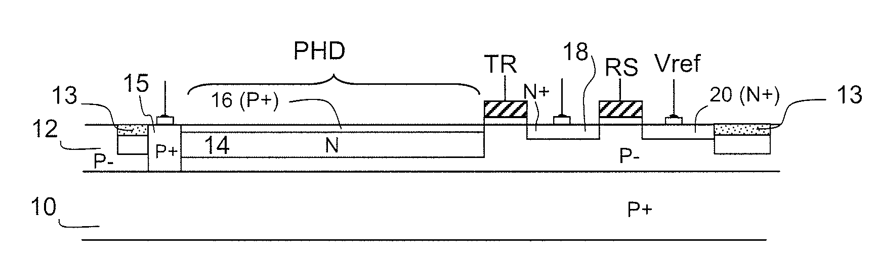
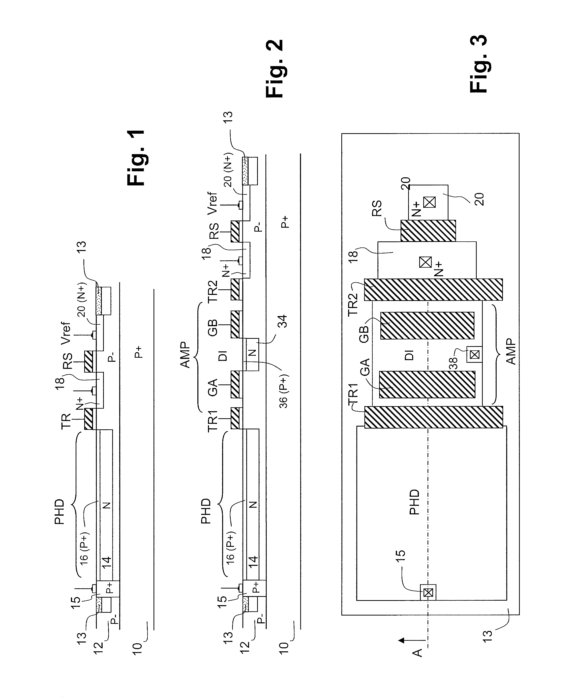
[0032]FIG. 1 shows the main elements of a conventional active pixel in CMOS technology. The pixel is formed in a substrate that preferably includes a lightly doped semiconductor active layer 12 of P− type (the symbol P− is used to denote this light doping) formed on the surface of a more heavily doped layer (P+). The pixel is isolated from the neighbouring pixels by an isolating barrier 13 that completely surrounds it. This barrier may be a surface isolating trench above a P-type well.

[0033]The pixel includes a photodiode region PHD, the perimeter of which follows the outline of an N-type semiconductor region implanted in part of the depth of the active layer 12. This implanted region is surmounted by a surface region 16 of P+ type, which is maintained at a zero reference potential. The photodiode is said to be “pinned” (the surface potential of the P+ surface region being fixed). The zero reference potential is that applied to the P− active layer. In the simplest case, this is the ...


PUM


Abstract

This description relates to active-pixel image sensors. Each pixel includes, at the surface of a semiconductor active layer, a photodiode region, a charge storage node and a transfer structure for transferring charges from the photodiode to the storage node after a charge integration time for charges generated by the light in the photodiode. The transfer structure includes a first transfer gate adjacent to the photodiode, a second transfer gate adjacent to the storage node, and an electron-multiplication amplifying structure located between the first and second transfer gates. The amplifying structure includes two separate accelerating gates and an intermediate diode region at a fixed surface potential, located between the two accelerating gates. A succession of alternating high and low potentials is applied to the accelerating gates while the charges are in transit in the transfer structure, before they are transferred to the storage node.

Description

RELATED APPLICATIONS[0001]The present application is based on, and claims priority from, French Application Number 1152413, filed Mar. 23, 2011, the disclosure of which is hereby incorporated by reference herein in its entirety.FIELD OF THE INVENTION[0002]The invention relates to image sensors, and more particularly those that are intended to collect images at low luminance levels and optionally also high luminance levels.BACKGROUND OF THE INVENTION[0003]When the light level is low, the pixels of a matrix image sensor collect few electrons. It is necessary to greatly increase the integration time in order to obtain an image, but this is to the detriment of the signal-to-noise ratio.[0004]In CCD (charge-coupled device) technology, it has already been proposed to incorporate, in a sensor, electron multiplication systems that create additional electrons from the electrons naturally generated by the light. The electrical signal which is then received is therefore multiplied by a factor....

Claims


Application Information

Patent Timeline
Patent Type & Authority Patents(United States)
IPC IPC(8): H01L27/148H01L27/146H04N5/351H04N5/3745
CPCH01L27/14612H04N5/351H04N5/3745H01L27/14603H04N25/50H04N25/77
Inventor FEREYRE, PIERREMAYER, FREDERIC
Owner TELEDYNE E2V SEMICON SAS
Why Eureka
Try Eureka