
Bit line and compare voltage modulation for sensing nonvolatile storage elements

a nonvolatile storage element and voltage modulation technology, applied in the field of bit line and compare voltage modulation for sensing nonvolatile storage elements, can solve the problems of programed word lines that often see low bit line resistance and represent an excessive use of power

Active Publication Date: 2015-07-14
SANDISK TECH LLC
View PDF44 Cites 63 Cited by
  • Summary
  • Abstract
  • Description
  • Claims
  • Application Information

AI Technical Summary

Benefits of technology

The patent text describes a method for programming non-volatile semiconductor memory devices, such as EEPROM and flash memory, using a floating gate to store data. The method involves applying a program voltage to the control gate of the memory cell and grounding the bit line. Electrons are injected into the floating gate to program the memory cell. The threshold voltage of the memory cell is raised by the amount of charge on the floating gate. The method includes multiple programming pulses and verification operations to ensure proper programming. The technical effect of the patent text is to provide a more efficient and effective method for programming non-volatile semiconductor memory devices.

Problems solved by technology

Earlier programmed word lines often see low bit line resistances during verify operations due to the fact that other word lines have not yet been programmed.
While this does not create a problem from a logic point of view, it can represent an excessive use of power.

Method used


Image

  • Bit line and compare voltage modulation for sensing nonvolatile storage elements
  • Bit line and compare voltage modulation for sensing nonvolatile storage elements
  • Bit line and compare voltage modulation for sensing nonvolatile storage elements

Examples


Embodiment Construction

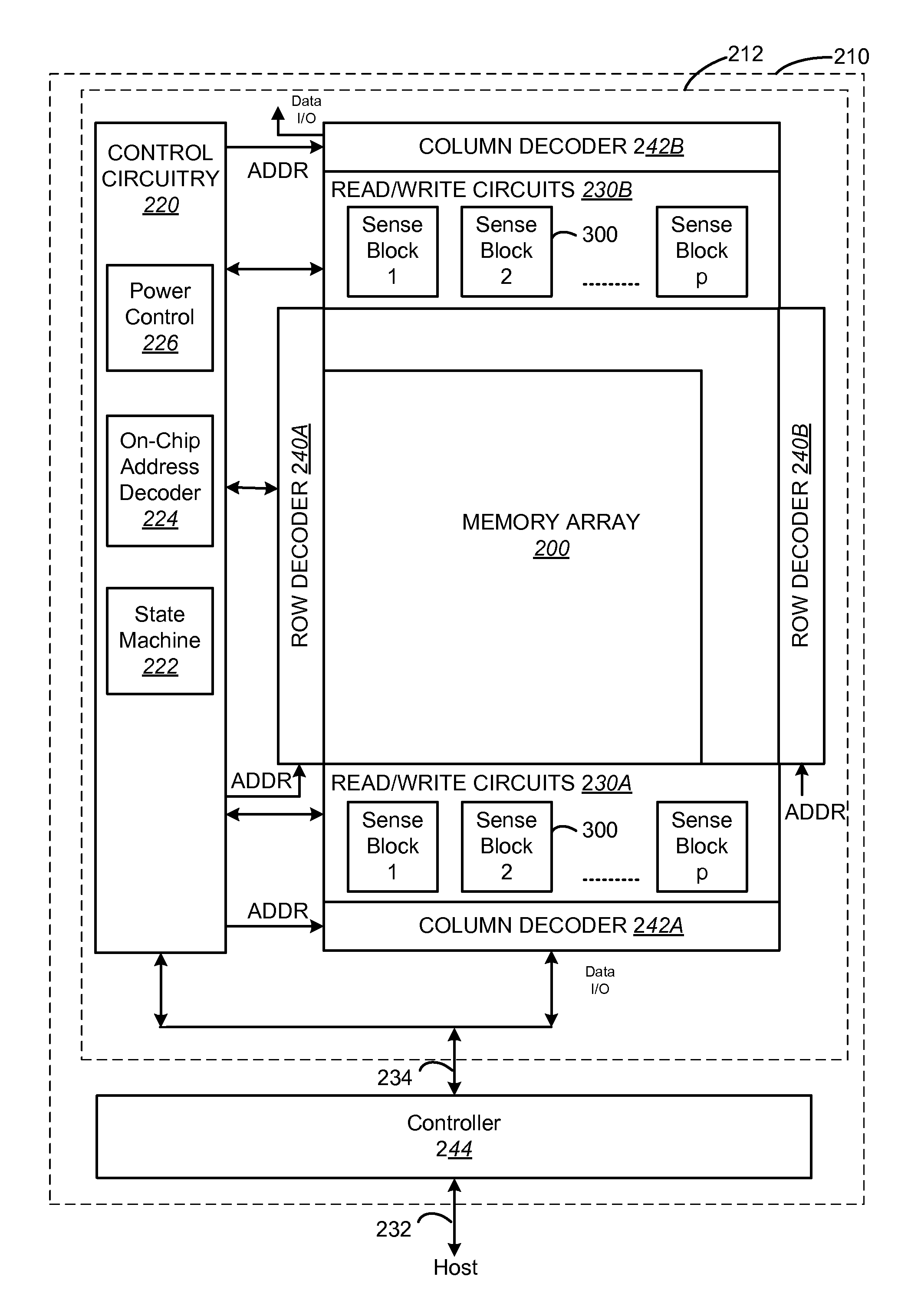
[0030]When memory cells connected to first programmed word lines conduct current in excess of the required threshold during sensing operations, these memory cells waste power. One way to conserve power during verify operations is to reduce the bit line voltage during verify operations for these first programmer word lines, thus bringing the current conducted by these memory cells closer to the required threshold. However, during the corresponding read operations of the first programmed word lines, not changing the corresponding bit line voltages can sometimes lead to an apparent decrease in threshold voltage of the memory cells. In one example implementation, to compensate for this apparent decrease in threshold voltage, one or more of the read bit line voltage, verify compare voltage, and / or read compare voltage can be adjusted.

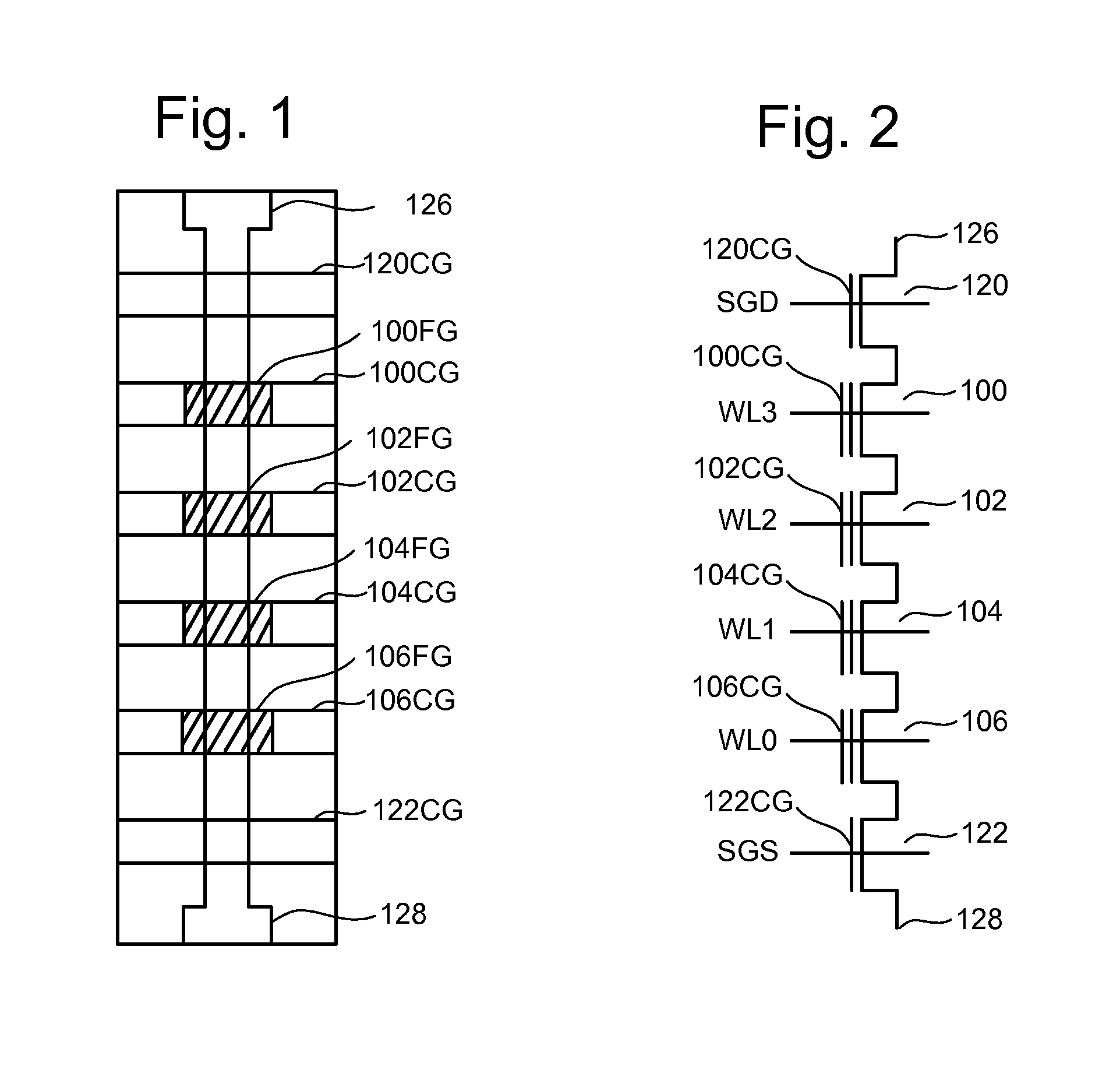
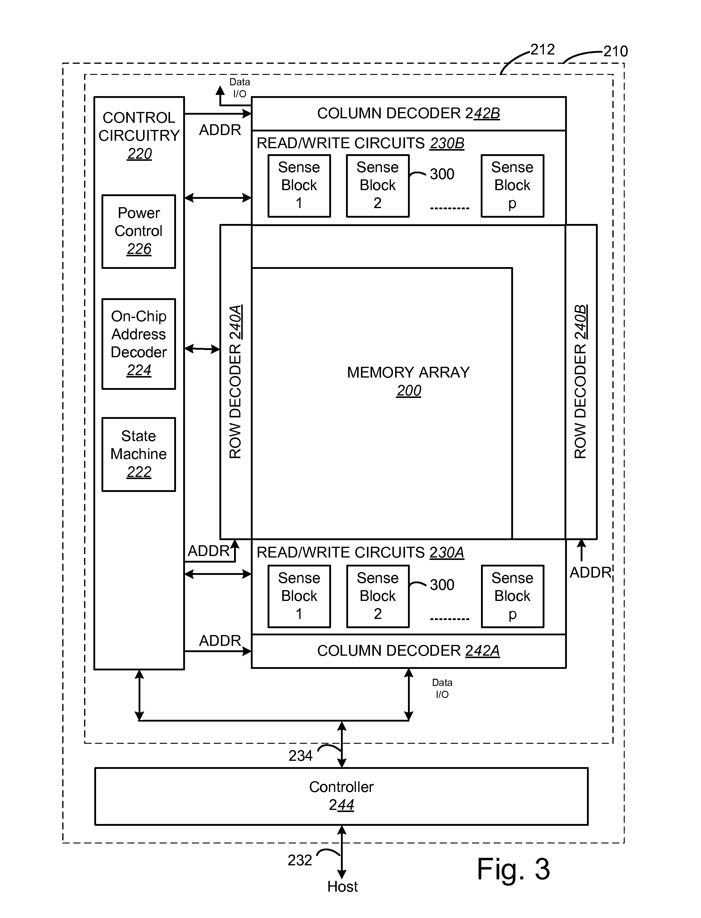
[0031]One example of a non-volatile storage system that can implement the technology described herein is a flash memory system that uses the NAND structure,...


PUM


Abstract

In a block of non-volatile memory, bit line current increases with bit line voltage. For current sensing memory systems, average bit line current during a sensing operation need only exceed a certain threshold amount in order to produce a correct result. For the first word lines being programmed in a block, memory cells connected thereto see relatively low bit line resistances during verify operations. In the disclosed technology, verify operations are performed for these first programmed word lines with lower verify bit line voltages in order to reduce excess bit line current and save power. During read operations, this scheme can make threshold voltages of memory cells connected to the lower word lines appear lower. In order to compensate for this effect, various schemes are disclosed.

Description

BACKGROUND OF THE INVENTION[0001]Semiconductor memory devices have become more popular for use in various electronic devices. For example, non-volatile semiconductor memory is used in cellular telephones, digital cameras, personal digital assistants, mobile computing devices, non-mobile computing devices and other devices. Electrical Erasable Programmable Read Only Memory (EEPROM) and flash memory are among the most popular non-volatile semiconductor memories.[0002]Both EEPROM and flash memory utilize a floating gate that is positioned above and insulated from a channel region in a semiconductor substrate. The floating gate is positioned between source and drain regions. A control gate is provided over and insulated from the floating gate. The threshold voltage of the transistor is controlled by the amount of charge that is retained on the floating gate. That is, the minimum amount of voltage that must be applied to the control gate before the transistor is turned on to permit condu...

Claims


Application Information

Patent Timeline
Patent Type & Authority Patents(United States)
IPC IPC(8): G11C16/04G11C11/56G11C16/34
CPCG11C16/3454G11C11/5628G11C11/5642G11C16/3459G11C7/12G11C16/24G11C16/26
Inventor DUNGA, MOHAN V.HIGASHITANI, MASAAKI
Owner SANDISK TECH LLC
Learn More