Semiconductor device including a counter layer, for power conversion and method of manufacturing the same

a technology of counter layer and semiconductor device, which is applied in the direction of semiconductor device, diode, electrical apparatus, etc., can solve the problems of loss of controllability of gate voltage, device destruction, and inability to control electron injection at the mos gate, so as to reduce the damage caused by process defects

Active Publication Date: 2015-07-14
FUJI ELECTRIC CO LTD
View PDF13 Cites 3 Cited by
  • Summary
  • Abstract
  • Description
  • Claims
  • Application Information

AI Technical Summary

Benefits of technology

[0062]In this manner, according to the present invention, with respect to an insulated gate semiconductor device such as an IGBT or a MOSFET, it is possible to provide a semiconductor device where switching destruction caused by process defects is reduced and a method of manufacturing the same.

Problems solved by technology

When the gate is in a turned-on state or at a turned-off time, if the latch-up occurs, the controllability of the gate voltage is lost, and in the worst case, the device may be destructed.
As a result, electron injection at the MOS gate may not be controlled.

Method used


Image

  • Semiconductor device including a counter layer, for power conversion and method of manufacturing the same
  • Semiconductor device including a counter layer, for power conversion and method of manufacturing the same
  • Semiconductor device including a counter layer, for power conversion and method of manufacturing the same

Examples


first embodiment

[0097](First Embodiment)

[0098]In a first embodiment, a MOS gate semiconductor device where a p-type counter layer is newly formed in order to prevent latch-up by suppressing pattern defect of a p-type contact layer formed on a surface of a p-type base layer and a method of manufacturing the same will be described.

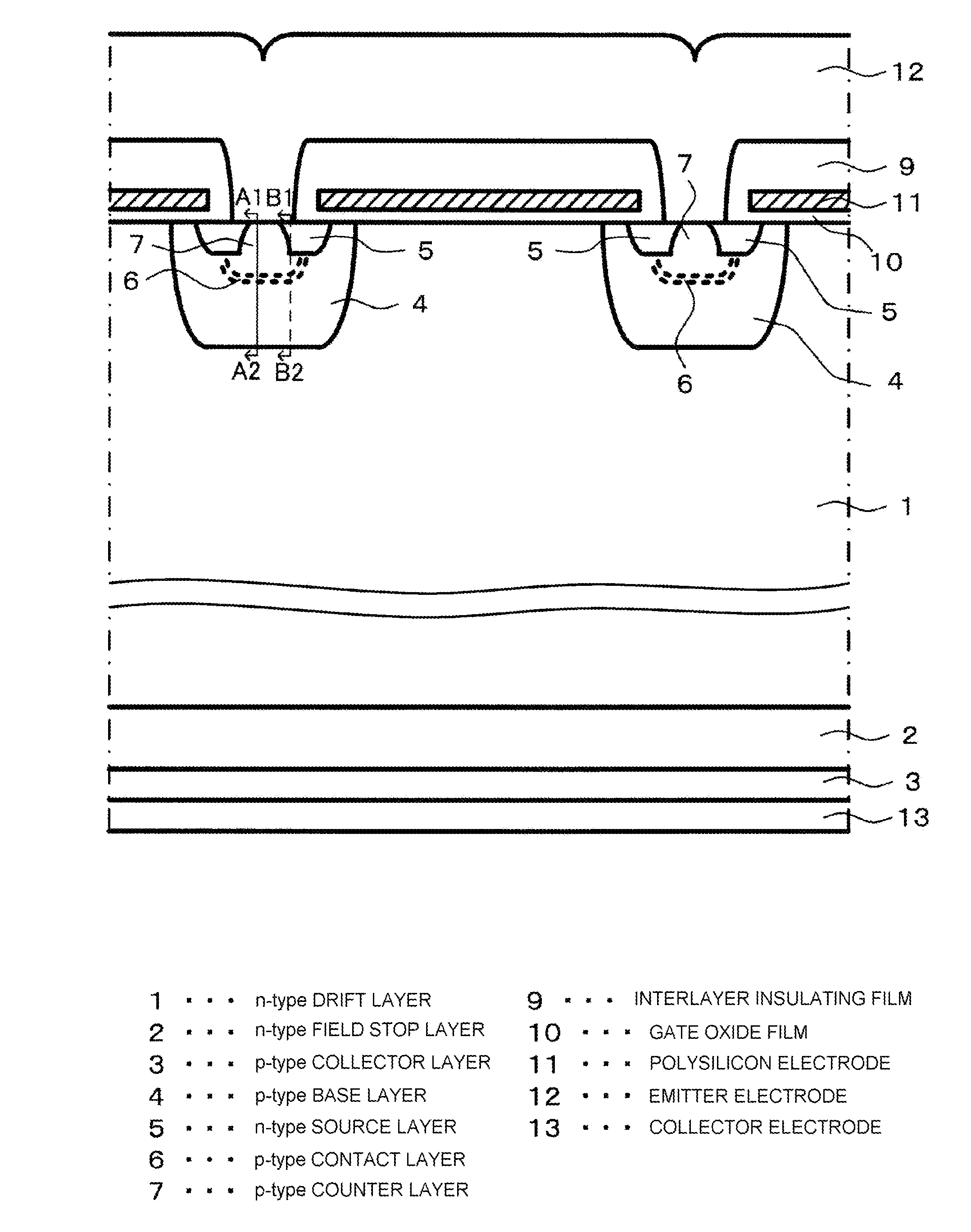
[0099]FIG. 1 is a cross-sectional view illustrating main components of a semiconductor device according to an embodiment of the present invention. FIG. 1 illustrates a cross-sectional view of an IGBT which is a semiconductor device according to the first embodiment. In FIG. 1, a p-type base layer 4 having a concentration higher than that of an n-type drift layer 1 is selectively formed on a surface of the semiconductor substrate including the n-type drift layer 1. An n-type source layer 5 having a concentration higher than that of the p-type base layer 4 is selectively formed on a surface of the p-type base layer 4. Moreover, a p-type contact layer 6 is formed in the p-type...

second embodiment

[0159](Second Embodiment)

[0160]Next, a second embodiment of the present invention will be described with reference to FIG. 9. FIG. 9 is a cross-sectional view illustrating main components of a semiconductor device according to an embodiment of the present invention and a concentration distribution diagram illustrating a net doping concentration of the semiconductor device. FIG. 9(a) illustrates a cross-sectional view of an IGBT as a semiconductor device according to the second embodiment of the present invention, and FIG. 9(b) illustrates net doping concentration distribution along cutting lines A1-A2 and B1-B2 illustrated in FIG. 9(a). In FIG. 9(b), the solid line indicates concentration distribution along the cutting line A1-A2, and the broken line indicates concentration distribution along the cutting line B1-B2.

[0161]The feature of the second embodiment is that the p-type counter layer 7 is formed so that the width thereof in the horizontal direction of the paper is almost equal...

fourth embodiment

[0171](Fourth Embodiment)

[0172]Next, a fourth embodiment of the present invention will be described with reference to FIG. 12. FIG. 12 is a cross-sectional view illustrating main components of a semiconductor device according to an embodiment of the present invention and a concentration distribution diagram illustrating a net doping concentration of the semiconductor device. FIG. 12(a) illustrates a cross-sectional view of an IGBT according to the fourth embodiment of the present invention, and FIG. 12(b) illustrates net doping concentration distribution along cutting lines A1-A2 and B1-B2 illustrated in FIG. 12(a). In FIG. 12(b), the solid line indicates concentration distribution along the cutting line A1-A2, and in FIG. 12(b), the broken line indicates concentration distribution along the cutting line B1-B2.

[0173]The feature of the fourth embodiment is that the depths of the p-type contact layer 6 and the p-type counter layer 7 are also different with respect to the third embodim...


PUM


Abstract

A p-type base layer is selectively formed on a surface of an n-type drift layer; an n-type source layer is selectively formed on a surface of the p-type base layer; and a p-type contact layer is formed to be in contact with the selectively-formed n-type source layer. A p-type counter layer is formed to be in contact with the n-type source layer, so as to overlap the p-type contact layer, so as to be separated from an interface where the p-type base layer and the gate oxide film are in contact with each other, and to be shallower than the p-type base layer. Accordingly, switching destruction caused by process defects in an insulated gate semiconductor device is reduced.

Description

TECHNICAL FIELD[0001]The present invention relates to a semiconductor device and a method of manufacturing the same, and more particularly, to a semiconductor device such as an insulated gate semiconductor device used for a power conversion apparatus such as an inverter for driving a motor and a method of manufacturing the same.BACKGROUND ART[0002]In the proceeding of low power consumption of a power conversion apparatus, low power consumption of a power device performing an important function in the power conversion apparatus has been demanded. Particularly, since an insulated gate transistor (MOSFET) or an insulated gate bipolar transistor (IGBT) of which gate can be driven by a voltage can be easily treated, application fields have been greatly widened.[0003]The MOSFET and the IGBT have a built-in parasitic structure. In other words, the MOSFET is a parasitic bipolar transistor (NPN structure), and the IGBT is a parasitic thyristor (PNPN structure). Particularly, in the case of t...

Claims


Application Information

Patent Timeline
Patent Type & Authority Patents(United States)
IPC IPC(8): H01L29/76H01L29/739H01L29/36H01L29/66H01L29/10H01L29/78H01L29/06H01L29/08
CPCH01L29/7395H01L29/1095H01L29/36H01L29/66712H01L29/7397H01L29/7802H01L29/0696H01L29/0847H01L29/0869H01L29/66333H01L21/266H01L27/0664H01L29/66325H01L2924/13055
Inventor ONOZAWA, YUICHISHIIGI, TAKASHI
Owner FUJI ELECTRIC CO LTD
Why Eureka
Try Eureka