Package substrate with current flow shaping features

Active Publication Date: 2015-11-10
ALTERA CORP
View PDF4 Cites 9 Cited by
  • Summary
  • Abstract
  • Description
  • Claims
  • Application Information

AI Technical Summary

Benefits of technology

[0004]Structures and techniques for making current densities in BGA contact pads for package substrates for semiconductor dies more uniform are discussed. Such structures and techniques may be primarily of interest with respect to power r

Problems solved by technology

Due to the costs involved in manufacturing semiconductor devices and various other factors, such devices are typically manufactured en masse on a semiconductor wafer, e.g., a silicon wafer.
Due to the fact such dice ar

Method used


Image

  • Package substrate with current flow shaping features
  • Package substrate with current flow shaping features
  • Package substrate with current flow shaping features

Examples


Embodiment Construction

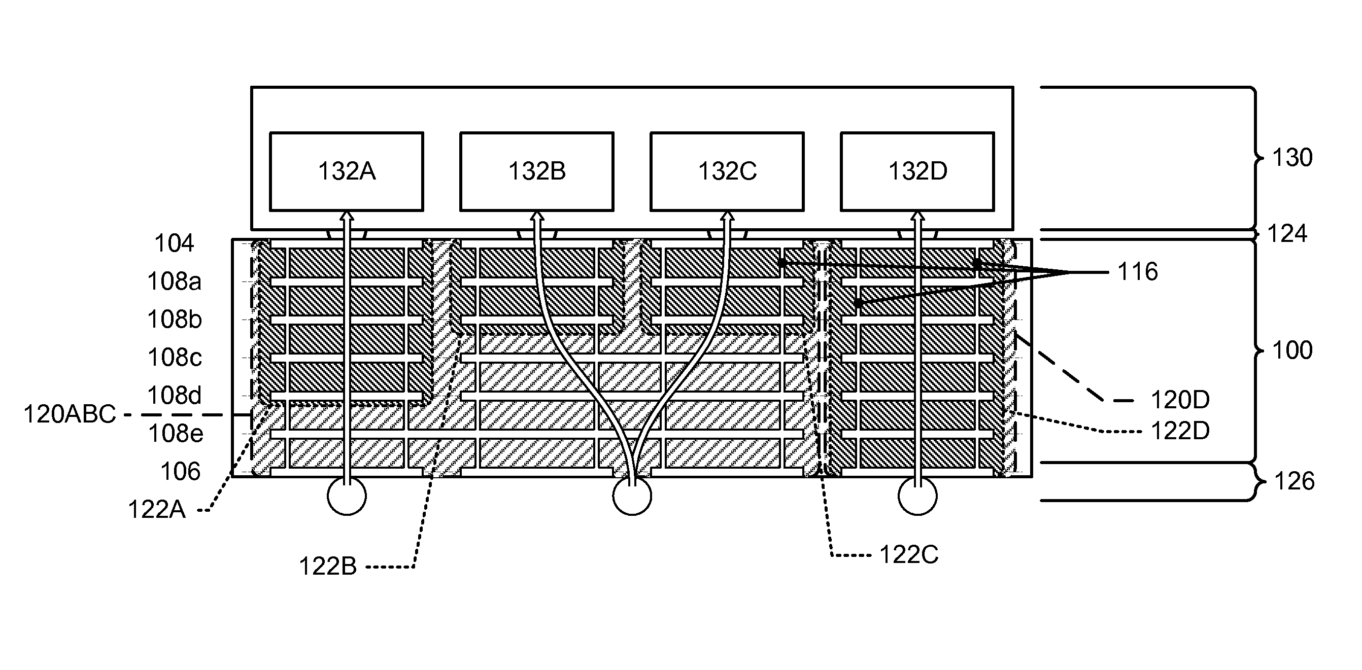
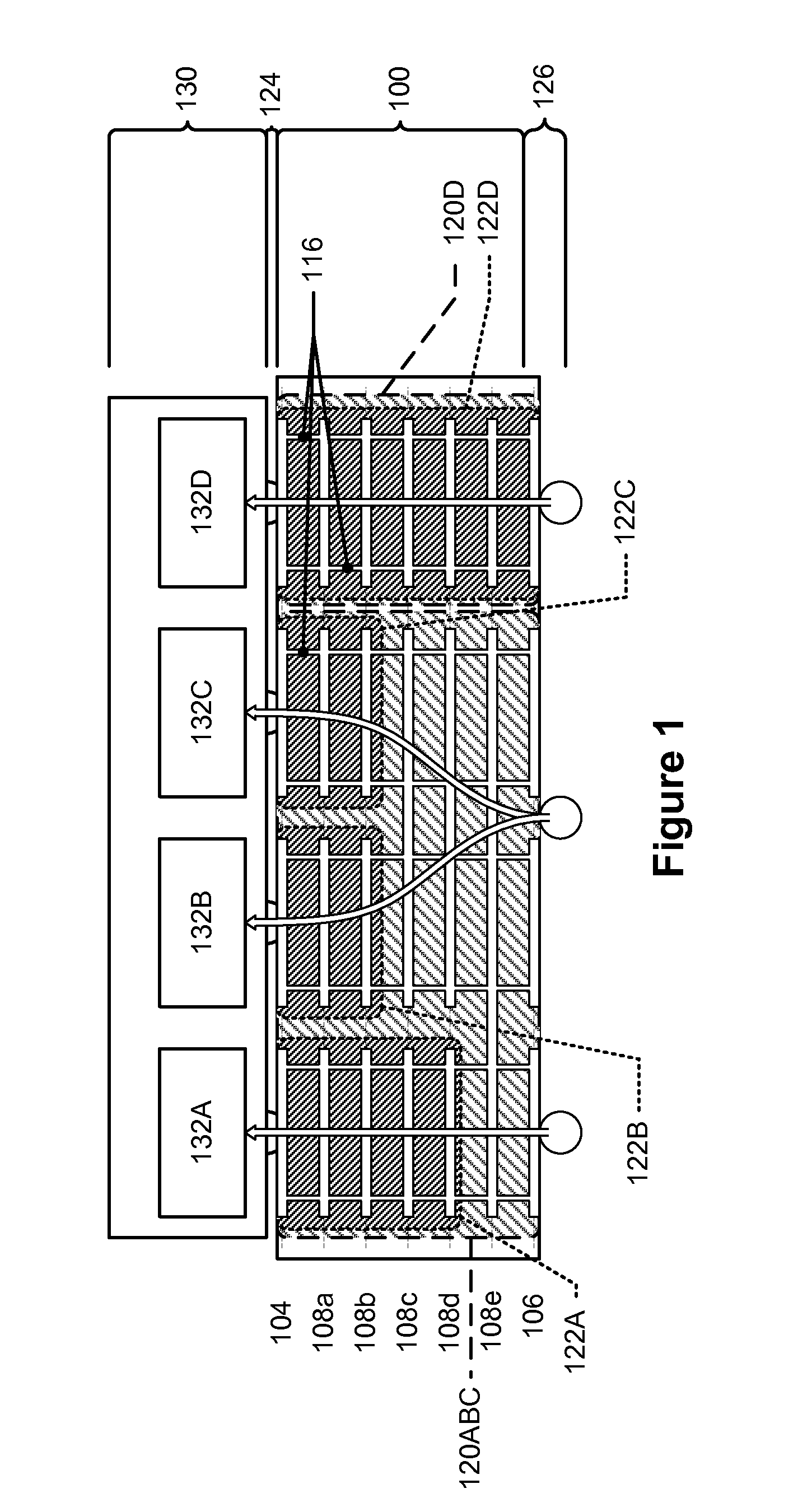
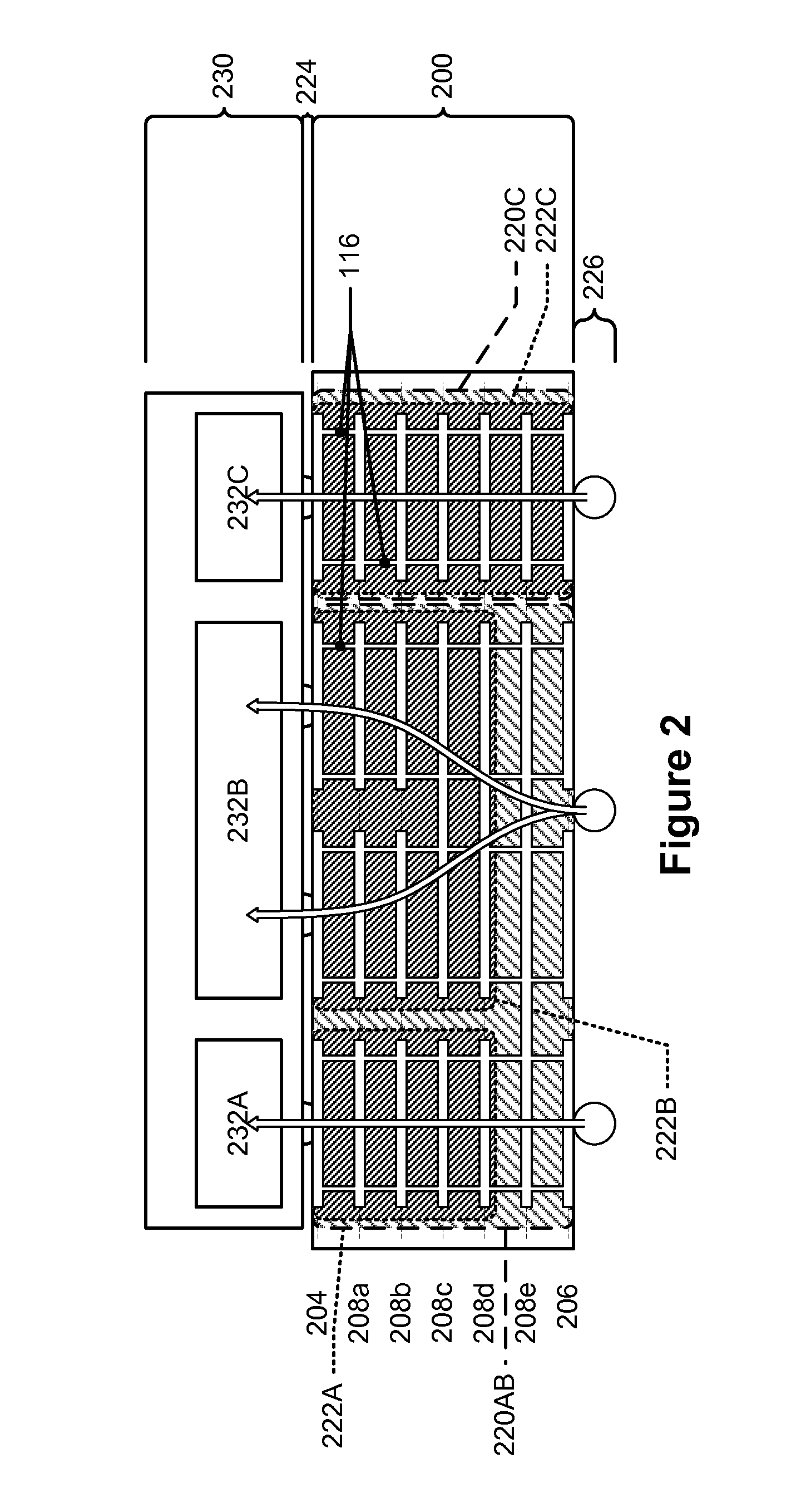
[0022]This disclosure relates to the design of package substrates for semiconductor packages. More specifically, this disclosure relates to techniques and structures that may be used in package substrate design to achieve a more uniform current density in, for example, BGA solder balls used to transmit core power to the semiconductor device through the package substrate.

[0023]Package substrates typically include a package core with a plurality of layers, each formed of a patterned conductive material. The layers are typically formed on a “package core,” which acts as a substrate upon which the layers may be deposited. The layers may be separated from one another by insulating layers (one of which may be the package core) to electrically isolate each layer from undesired electrical contact with the other layers. As used herein, the general term “layer” refers to a layer formed of patterned conductive material, whereas the term “insulating layer” is used to refer to a layer made of in...


PUM


Abstract

Techniques and structures for achieving a more uniform current density in solder ball contact areas for a ball-grid-array semiconductor package are presented. Current density may be made more uniform by introducing electrically non-conductive regions into one or more areas that form a dedicated power rail within a package substrate that is configured to be connected with a die. Additionally or alternatively, the number of μvias that connect each solder ball contact area with conductive areas within the package substrate may be individually tailored based on the desired current density at each solder ball contact area.

Description

BACKGROUND OF THE INVENTION[0001]Due to the costs involved in manufacturing semiconductor devices and various other factors, such devices are typically manufactured en masse on a semiconductor wafer, e.g., a silicon wafer. A single silicon wafer may hold hundreds or thousands of semiconductor devices. After semiconductor processing operations are complete, the wafer may be cut apart, or “diced,” to separate the individual semiconductor devices. The resulting semiconductor devices are called “dice,” or, in the singular, a “die.”[0002]Due to the fact such dice are quite fragile and have feature sizes that are still quite small, it is common practice to affix a die to a package substrate to form a semiconductor package which is then sold to manufacturers of electronic devices. The package substrate is larger than the die in area and provides, among other things, structural support to the die as well as an electrical interface that serves to connect electrical contacts on the die side w...

Claims


Application Information

Patent Timeline
IPC IPC(8): H01L23/498H01L23/50H01L27/02G06F17/50H01L23/538H01L23/532
CPCH01L27/0207H01L23/49816H01L23/49827H01L23/50G06F17/5072H01L23/53285H01L23/5385H01L23/49822H01L23/49838H01L2924/0002G06F30/398G06F30/394H01L2924/00G06F30/392
Inventor LIU, HUI
Owner ALTERA CORP
Why Eureka
Try Eureka