Low power ADC for high dynamic range integrating pixel arrays

a high dynamic range, pixel array technology, applied in analogue/digital conversion, color television details, television systems, etc., can solve the problems of difficult to achieve very large charge capacity in small pixel pitch, analog circuits that do not scale well, and increase transistor noise for smaller pixel pitch, so as to reduce csc capacitance and reduce charge reset noise

Active Publication Date: 2015-11-24
BFE ACQUISITION SUB II LLC D B A BLACK FOREST ENG
View PDF3 Cites 19 Cited by
  • Summary
  • Abstract
  • Description
  • Claims
  • Application Information

AI Technical Summary

Benefits of technology

[0015]A second capacitor is termed a step charge capacitor (CSC), and has a first node connected to a step voltage clock øSTEP and a second node connected to a step charge node. A step charge subtractor circuit is connected between the step charge node and integration node with an insolation transistor controlled by a voltage Vs. A state latch sends a signal to the state charge subtractor to subtract a fixed amount of charge from the integration node. The step clock voltage, øSTEP, is typically much larger than the ROIC analog supply voltage (˜3.3-5.0 volts). Large øSTEP amplitude allows a significant reduction in CSC capacitance for a fixed amount of step charge and a significant reduction in charge reset noise (related to kTCSC).

Problems solved by technology

One serious limitation of current ROIC technology is the difficulty of achieving very large charge capacity in small pixel pitch.
Analog circuits do not scale well because voltages and capacitances are reduced and transistor noise increases for smaller technologies and sizes.
There have been efforts to overcome these analog limitations by implementing an A / D converter in each pixel, but those we are aware of have significant problems with high noise, large power dissipation and require extremely expensive non-recurring costs for very small design rule CMOS tooling.
The ADC per pixel concept (also referred to as a digital pixel sensor (DPS)) has increased difficulty of implementation in large format mega-pixel FPAs as pixel pitch is reduced (14-bits) and FPA frame rate is increased (>60 Hz).
The repeated voltage reset or charge reset of CINT adds additional temporal noise.

Method used


Image

  • Low power ADC for high dynamic range integrating pixel arrays
  • Low power ADC for high dynamic range integrating pixel arrays
  • Low power ADC for high dynamic range integrating pixel arrays

Examples


Embodiment Construction

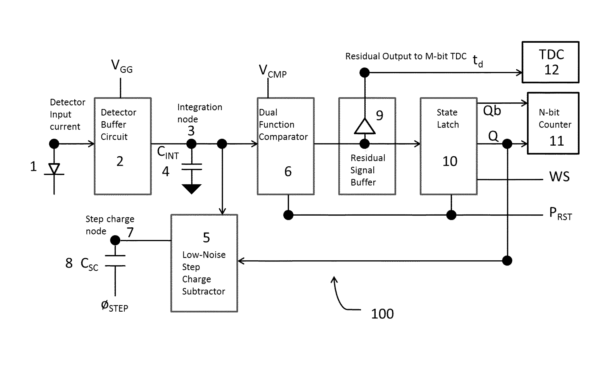
[0028]Disclosed herein is a low power two-step ADC, such as one that may be used in a large imaging array. An exemplary embodiment is depicted in FIG. 4. A low power two-step ADC 100 is connected by a detector buffer circuit 2 or other signal conditioning circuitry to detection components, represented as a diode 1. An input integration node 3 is a point at which current from the detector enters the circuit 100 substantially unchanged by the circuit 100. An integrating capacitor 4, a step charge subtractor 5 and a dual function comparator 6 are each connected in parallel to the integration node 3.

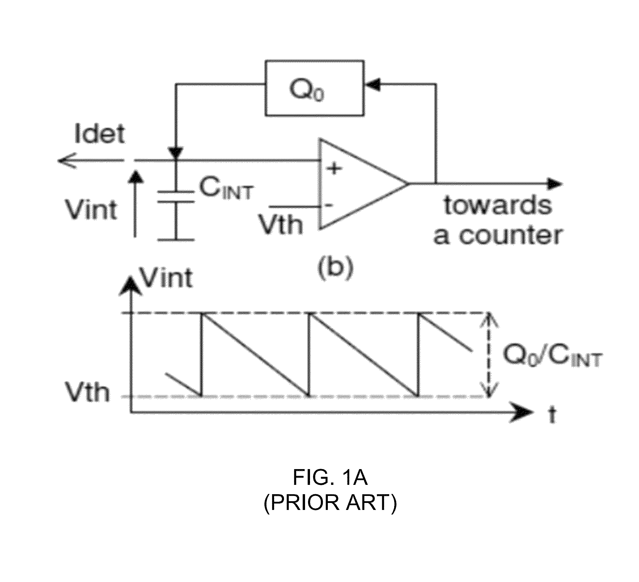
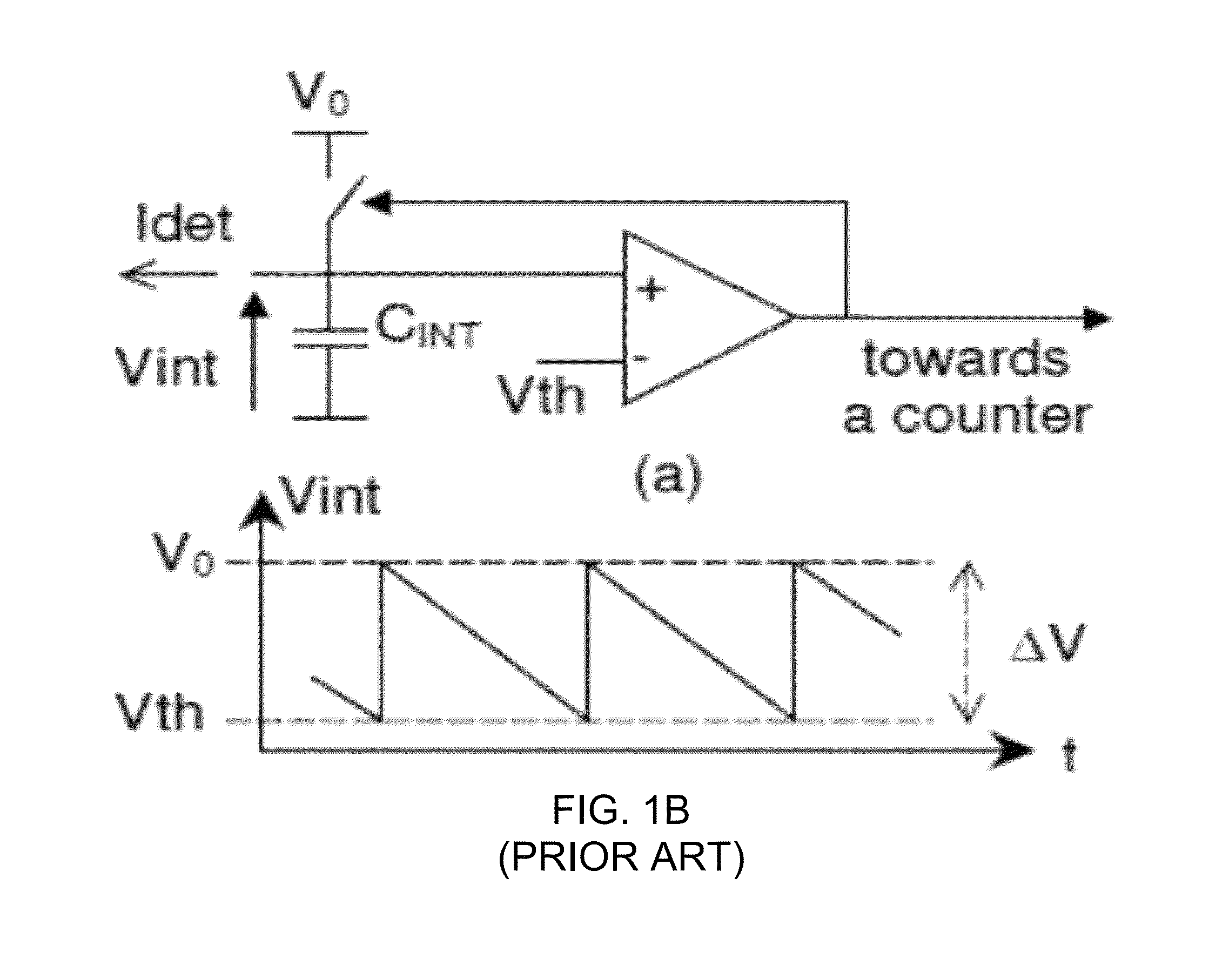
[0029]The detector buffer circuit 2 isolates the detector from the charge integration node 3 which is dominated by capacitor CINT. In some cases, such as a detector with large reverse bias capability, a detector buffer circuit is not required and charge integration can occur directly on the detector capacitance. The most simple detector buffer circuit is am input transistor comprising a low ...


PUM


Abstract

In one or more embodiments, an apparatus and method for processing an analog signal into a digital signal includes an input current buffer circuit, a signal charge integration node, a dual function comparator, a step charge subtractor, a state latch, a coarse N-bit counter, an optional residue signal buffer and a residue signal M-bit time-to-digital (TDC) converter. The circuitry is free running, meaning that it is never reset. Instead, what is tracked for each frame is how much additional charge has been accumulated since the end of the previous integration period. Between each frame, the state of the counter and the amount of charge residing in the integration node are recorded. This information from the beginning and end of a given frame is differenced and to this is added the amount of charge indicated by the number of times the counter overflowed during the integration period.

Description

CROSS-REFERENCE TO RELATED APPLICATION[0001]This application claims the benefit of U.S. Provisional Application No. 61 / 884,601, filed 30 Sep. 2013.STATEMENT REGARDING FEDERALLY SPONSORED RESEARCH OR DEVELOPMENT[0002]This invention was made with Government support under SBIR contract No. HQ0147-12-C-7808 awarded by the Missile Defense Agency. The Government has certain SBIR Data rights in this invention.TECHNICAL FIELD OF THE INVENTION[0003]The teachings herein relate to a low power analog to digital conversion (ADC) that is particularly advantageous for use with sensors of an array.BACKGROUND OF THE INVENTION[0004]Advanced focal plane arrays (FPAs), such as infrared focal plane arrays (IRFPAs) utilize embedded ADCs on the read out integrated circuitry (ROIC) die. On-ROIC digital readout allows on-chip digital signal processing, increased dynamic range, and increased signal to noise ratio. On-ROIC ADC is often incorporated at one or more FPA outputs or at ROIC columns. More ADCs on t...

Claims


Application Information

Patent Timeline
Patent Type & Authority Patents(United States)
IPC IPC(8): H03M1/12H04N5/365H04N5/378
CPCH03M1/12H04N5/3653H04N5/378H03M1/44H03M1/50H04N25/65H04N25/772H04N25/75H04N25/672
Inventor GAALEMA, STEPHENBAHN, WILLIAMDOBYNS, DAVIDTRAN, TUE
Owner BFE ACQUISITION SUB II LLC D B A BLACK FOREST ENG
Why Eureka
Try Eureka