Method and apparatus of electrical property measurement using an AFM operating in peak force tapping mode

a technology of peak force tapping and electrical property measurement, which is applied in the field of scanning probe microscopy methods and apparatuses, can solve the problems of poor spatial resolution, spm limits the possible q value, and the sensitivity of kpfm is thereby necessarily limited, and achieves improved accuracy/resolution and high performance.

Active Publication Date: 2015-12-15
BRUKER NANO INC
View PDF75 Cites 2 Cited by
  • Summary
  • Abstract
  • Description
  • Claims
  • Application Information

AI Technical Summary

Benefits of technology

[0039]The preferred embodiments are directed to high performance KPFM. More particularly, the invention is directed to an AFM that combines mechanical property measurement of a sample, e.g., on the nanoscale, with the capability to characterize electrical properties using a Kelvin probe configuration. The preferred embodiments make it possible to measure mechanical properties and electrical properties of a sample at the same time, with improved accuracy / resolution, at the nanometer scale, and associate that electrical property data with more credible topography and mechanical property information concerning the sample.
[0040]By employing an innovative mode of AFM operation, peak force tapping mode (PFT mode), the exemplary embodiments are able to achieve higher sensitivity factor as well as accuracy / repeatability improvements over known systems, primarily due to PFT mode's ability to support probes having higher sensitivity factor. Moreover, the exemplary embodiments combine the mechanical and electrical capabilities of AFM to substantially fully characterize samples on, e.g., the nanometer scale. While PFT methods and apparatus operate to gather data concerning mechanical properties of a sample and KPFM methods and apparatus operate to gather data concerning electrical properties of a sample, the preferred embodiments make AFM more powerful by integrating the two together. Not only does the result improve user efficiency, but also allows in situ correlation of mechanical properties and electrical properties for very small features (i.e., high resolution), thus providing new information regarding a material's characteristics and performance.
[0041]Preferably, the probe of the exemplary embodiments has a tip including a body made of a homogeneous material (conducting) from its base to its apex. Homogeneous material means the same chemical composition, physical properties (including conductivity), crystalline orientation and surface potential. In one embodiment, the tip is made of a homogeneous conducting material, with an insulating layer between the cantilever and tip base. The insulating layer can be optional but the homogeneous material of the tip (base to apex) must always be present. In an alternative embodiment, the tip and the cantilever are made of one homogeneous material that is conducting. Using either of these embodiments of the probe, the accuracy of the present KPFM measurement is substantially improved.

Problems solved by technology

Traditional Kelvin probe technique has a high sensitivity for potential measurements but offers poor spatial resolution.
One of the challenges with KPFM, FM-KPFM mode in particular, is that a low spring constant and high cantilever Q is desirable for making sensitive high resolution measurements.
However, though one of the major advantages of SPM over other high-resolution microscopes (such as SEM) is operation in air, SPM limits possible Q values.
However, for practical reasons (e.g., to help prevent the probe tip from sticking to the sample as it makes intermittent contact therewith), TappingMode requires use of probes having relatively high spring constants for reliable operation; and not too high a Q value to attain a bandwidth that allows a reasonably fast scan rate.
KPFM sensitivity is thereby necessarily limited.
Contact mode permits the use of levers having lower spring constants but is generally known to be one of the most destructive SPM techniques and is therefore limited with respect to which the types of samples with which it can be used.
KPFM accuracy and resolution can also be limited by any one or more of the following: tip wear, tip contamination (need stable tip work function), metal degradation particularly over the apex, parasitic capacitance (compromise lateral resolution), parasitic electrochemistry, unintentional charge dissipation from the sample, etc.
In the end, notwithstanding the broad application and capabilities of AFM and KPFM, limitations with each have remained.
Sensitivity is the primary limitation of KPFM.
However, while AFM is reliable in providing multidimensional information with very high resolution and has gained broad acceptance as the tool of choice for many applications in imaging (e.g., topography), AFM has not been as successful with respect to quantitative mechanical property characterization.
Another fundamental limitation of current KPFM is that it is integrated with Tapping Mode (or intermittent contact mode or AC mode).
Using probes having a much lower spring constant is therefore desirable; however, low spring constant probes are incompatible with the requirements of Tapping Mode feedback stability.
More particularly, conventional AFM has been known for its inability to simultaneously acquire both high-resolution images and quantitative mechanical property information (e.g., elasticity, plasticity, and adhesion).
Measuring mechanical properties with an AFM experimental setup is possible, but most known methods and systems rely on collecting force curves corresponding to the local tip-sample interaction, an extremely slow process.
Additionally, current KPFM measurement systems are subject to large variations in the surface potential value, due primarily to changes at the probe apex during imaging.
Drift can be substantial, often exceeding hundreds of mV, thereby making accurate measurements using AFM impractical.
These changes are typically caused by uncertainty and variation of the conductive coating on the AFM probe; in particular, the crystal structure of the apex of the tip is poorly defined and changes from probe to probe.
In either case, the KPFM measurement is compromised.

Method used


Image

  • Method and apparatus of electrical property measurement using an AFM operating in peak force tapping mode
  • Method and apparatus of electrical property measurement using an AFM operating in peak force tapping mode
  • Method and apparatus of electrical property measurement using an AFM operating in peak force tapping mode

Examples


Embodiment Construction

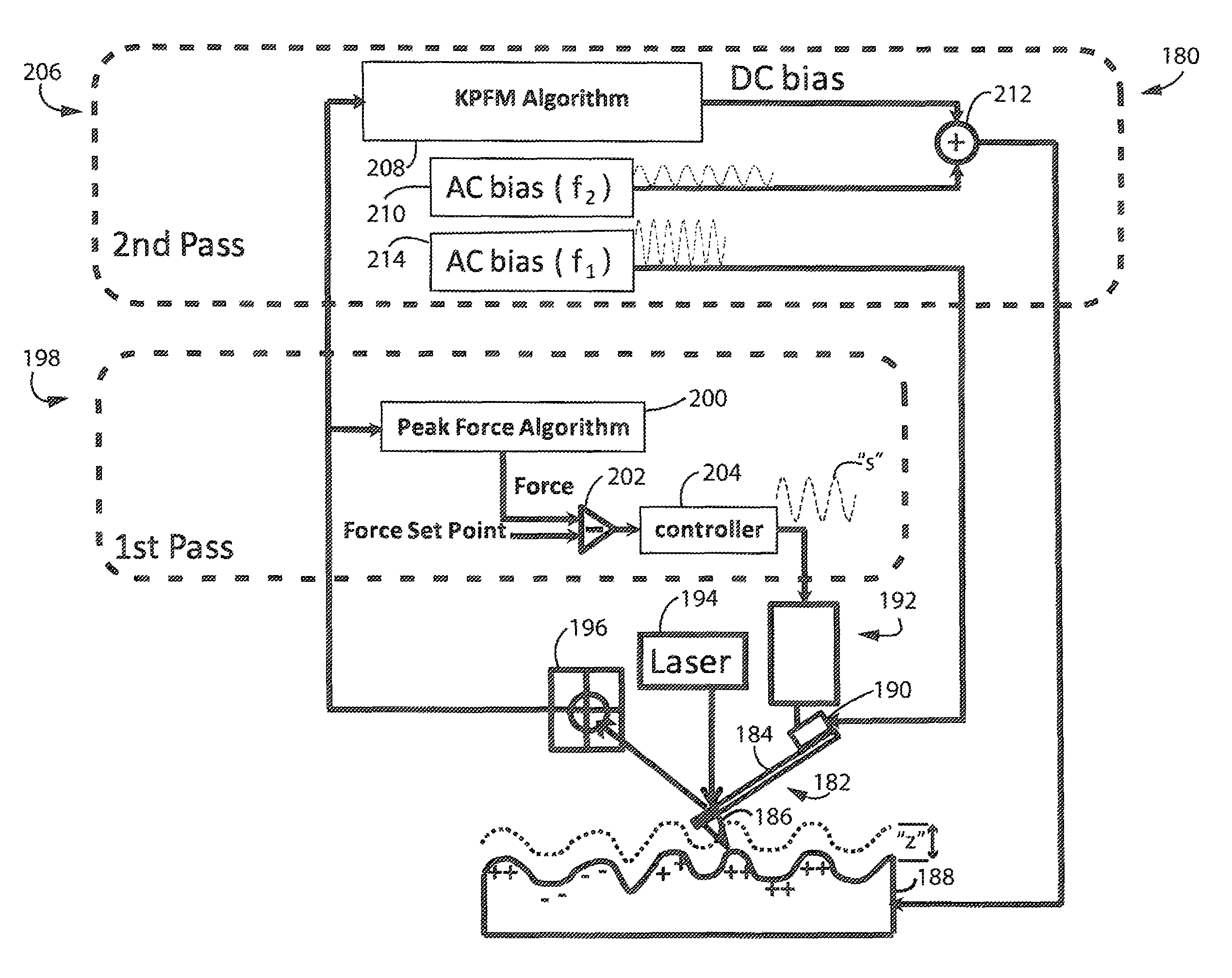
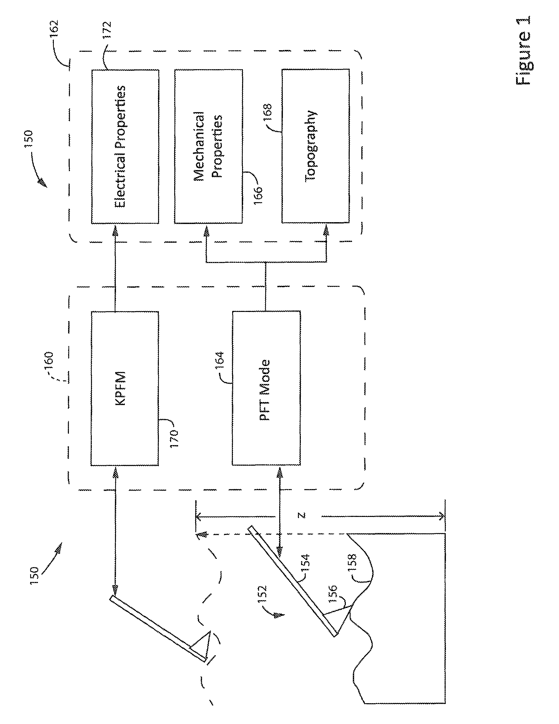
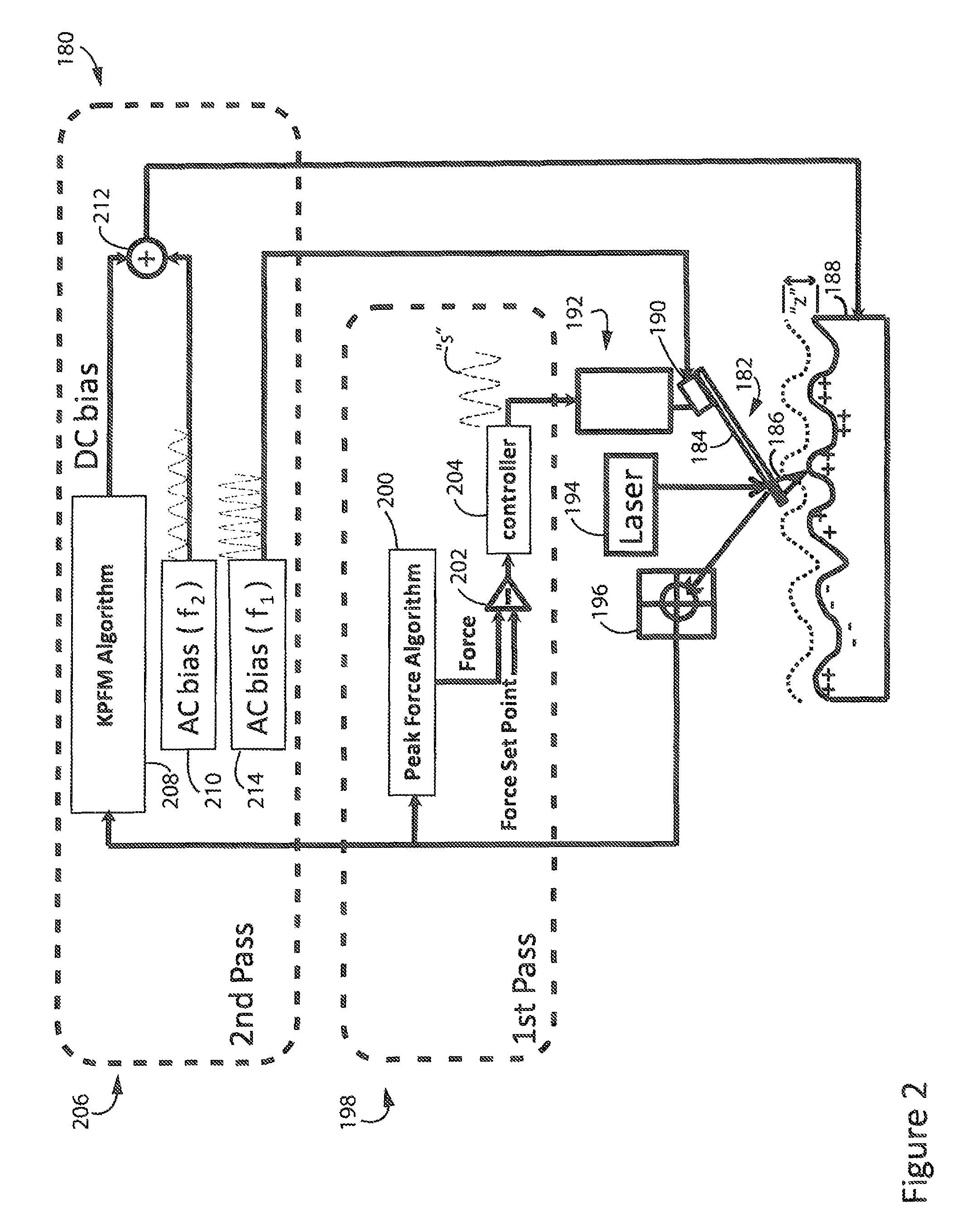
[0075]The benefits of PFT mode AFM are numerous. Most noteworthy is its capability of simultaneous quantitative mechanical property mapping and topographical imaging. Moreover, its ability to use cantilevers having properties (spring constant, resonant frequency and quality factor) over a wide range allows for probe selection most suited to KPFM operation. It is the object of this invention to combine PFT mode AFM with KPFM, preferably FM-KPFM, and AM-KPFM as an alternative. This will offer simultaneous surface topography, mechanical properties, and surface potential (electrical property) mapping with enhanced sensitivity. Ease-of-use operation also benefits beginner users for getting high quality data without intensive learning and practicing. The implementation and benefits will be outlined below.

[0076]Peak Force Tapping Mode (PFT mode), provides a solution to the quantitative mechanical property mapping. With the tip driven in and out of the contact with the surface at multi-kilo...


PUM


Abstract

An apparatus and method of collecting topography, mechanical property data and electrical property data with an atomic force microscope (AFM) in either a single pass or a dual pass operation. PFT mode is preferably employed thus allowing the use of a wide range of probes, one benefit of which is to enhance the sensitivity of electrical property measurement.

Description

CROSS-REFERENCE TO RELATED APPLICATIONS[0001]This application is a non-provisional application claiming priority to Provisional Patent Application Ser. No. 61 / 663,528, filed on Jun. 22, 2012, entitled Method and Apparatus of Electrical Property Measurement Using an AFM Operating in Peak Force Tapping Mode. It is also a continuation-in-part of and claims priority to U.S. Non-Provisional patent application Ser. No. 13 / 306,867, tiled on Nov. 29, 2011, which claims priority to Provisional Patent Application Ser. No. 61 / 417,837, filed on Nov. 29, 2010, both entitled Method and Apparatus of Using Peak Force Tapping Mode to Measure Physical Properties of a Sample, and is also a continuation-in-part of U.S. patent application Ser. No. 12 / 618,641, filed on Nov. 13, 2009, entitled Method and Apparatus of Operating a Scanning Probe Microscope, which in turn, claims priority under 35 USC §1.119(e) to U.S. Provisional Patent Application Ser. No. 61 / 114,399, filed Nov. 13, 2008. The subject matte...

Claims


Application Information

Patent Timeline
Patent Type & Authority Patents(United States)
IPC IPC(8): G01Q60/24G01Q60/30G01Q20/00G01Q60/34G01Q20/02G01Q60/32B82Y35/00G01Q10/06
CPCG01Q20/00B82Y35/00G01Q10/065G01Q20/02G01Q60/30G01Q60/32G01Q60/34G01Q60/00G01Q60/24
Inventor LI, CHUNZENGHU, YANMA, JIHE, JIANLIHUANG, LINMINNE, STEPHEN C.MITTEL, HENRYWANG, WEIJIEHU, SHUIQINGSU, CHANMIN
Owner BRUKER NANO INC
Why Eureka
Try Eureka