Apparatus and method of forming an indium gallium zinc oxide layer

a technology of indium gallium zinc oxide and thin film transistor, which is applied in the direction of transistors, chemical vapor deposition coatings, coatings, etc., can solve the problems of limiting the development of pvd igzo process, being more expensive in production than a single-chamber process, and being susceptible to environmental degradation

Active Publication Date: 2015-12-15
APPLIED MATERIALS INC
View PDF7 Cites 172 Cited by
  • Summary
  • Abstract
  • Description
  • Claims
  • Application Information

AI Technical Summary

Problems solved by technology

However, the formation of an IGZO layer has its own set of challenges.
This not only limits PVD IGZO process development, but limits a PVD deposited IGZO containing structure to a single layer having either a 5:1:1 composition or a 1:1:1 composition, or to a bi-layer structure, where one film has 5:1:1 composition and the other has a 1:1:1 composition.
Finally, a PVD bi-layer process requires two separate PVD chambers, which is more expensive in production than a single-chamber process.
Another problem with IGZO films is their susceptibility to environmental degradation, reported as the diffusion of hydrogen atoms into the IGZO active layer which affects transistor properties.

Method used


Image

  • Apparatus and method of forming an indium gallium zinc oxide layer
  • Apparatus and method of forming an indium gallium zinc oxide layer
  • Apparatus and method of forming an indium gallium zinc oxide layer

Examples


Embodiment Construction

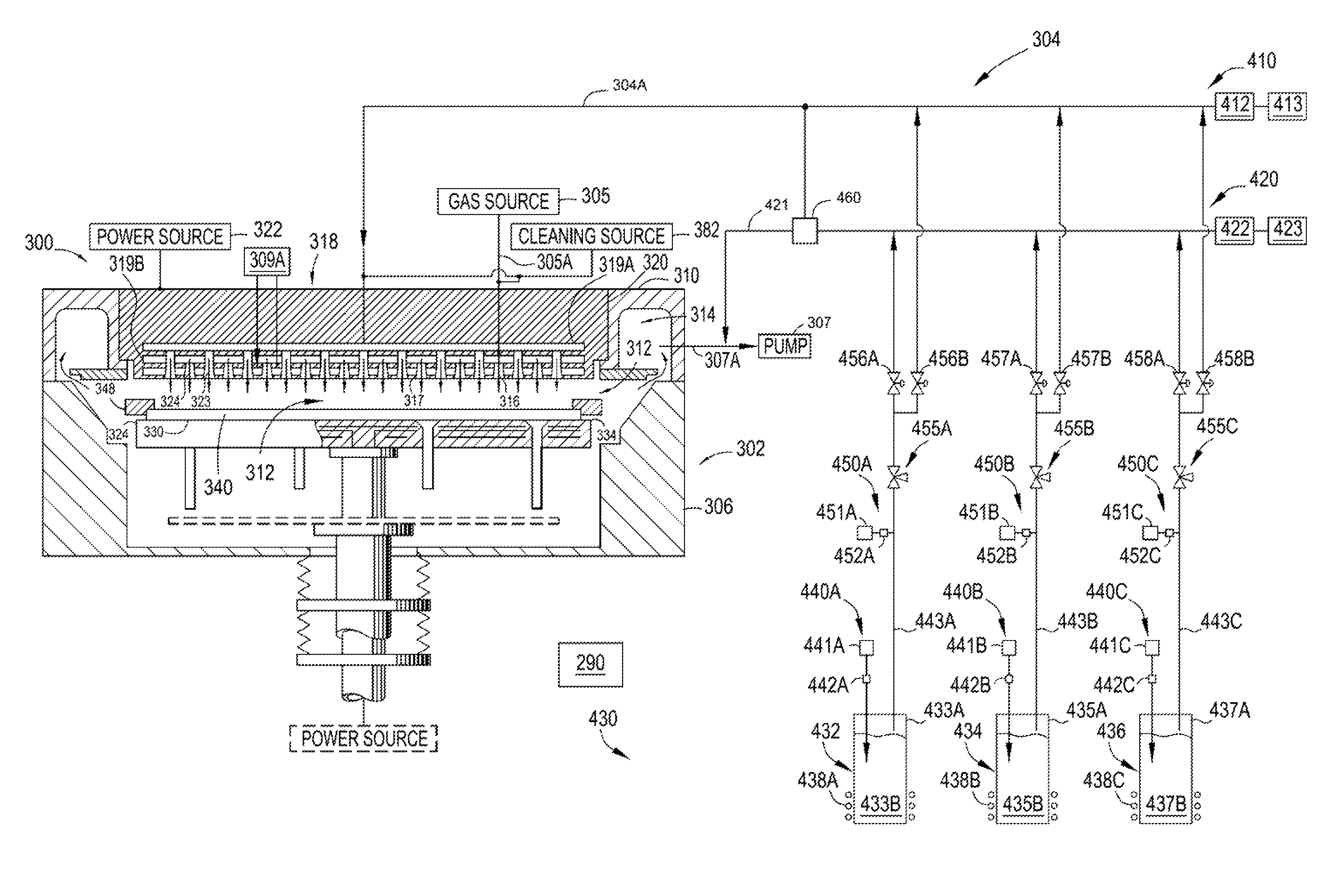
[0023]The embodiments of the disclosure may provide a method and apparatus for forming a thin film transistor (TFT) device that includes an indium gallium zinc oxide (IGZO) layer. The embodiments of the disclosure are illustratively described below in reference to a plasma enhanced chemical vapor deposition system configured to form an IGZO layer on large area substrates, such as a plasma enhanced chemical vapor deposition (PECVD) system, available from AKT, a division of Applied Materials, Inc., Santa Clara, Calif. However, it should be understood that the embodiments disclosed herein have utility in other system configurations, such as other types of chemical vapor deposition systems and other systems that are configured to distribute a multi-component precursor gas to and within a process chamber, including those systems configured to process round substrates.

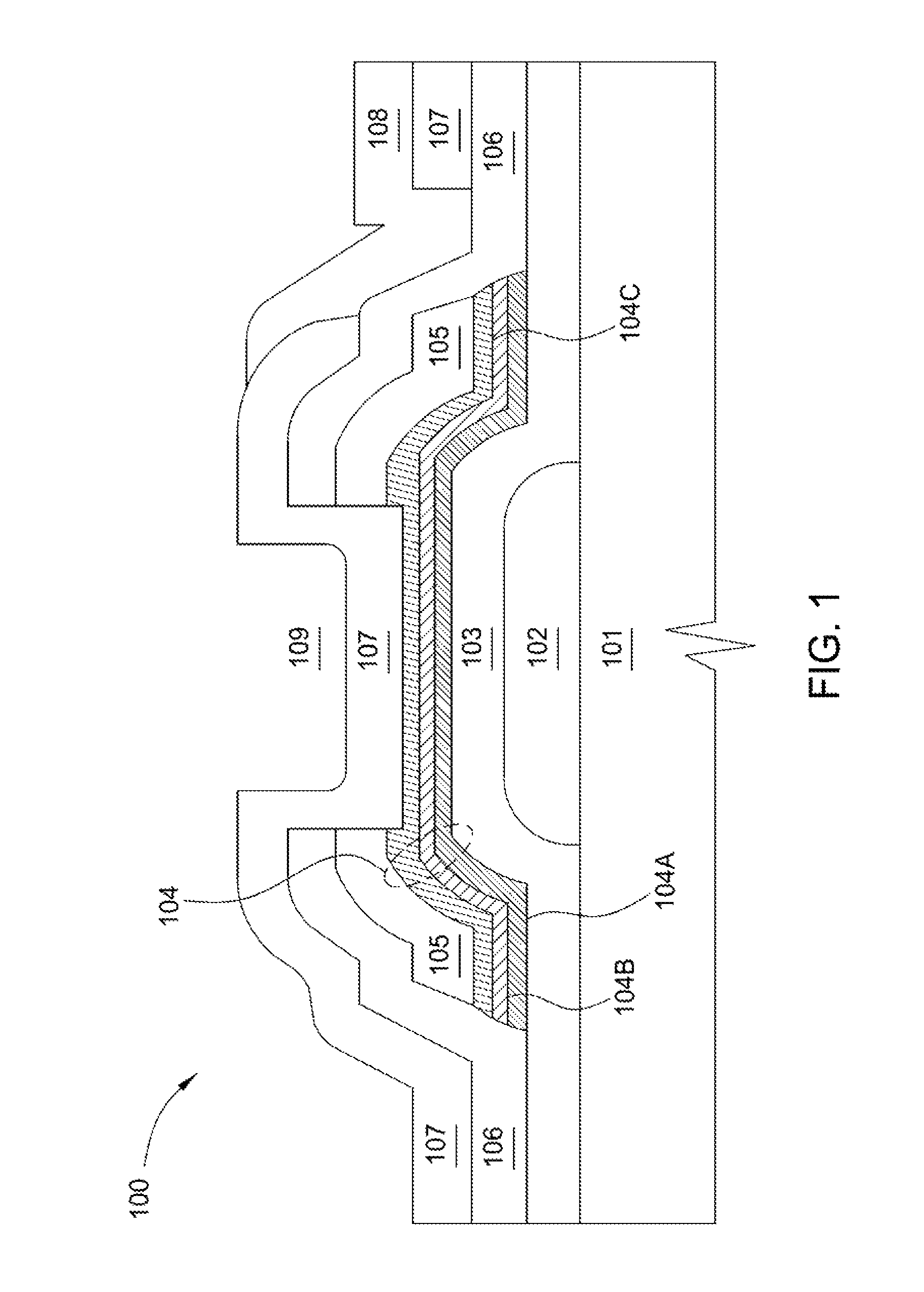
[0024]FIG. 1 illustrates cross-sectional schematic views of a thin film transistor structure 100. The substrate 101 may co...


PUM

PropertyMeasurementUnit
surface areaaaaaaaaaaa
temperatureaaaaaaaaaa

Abstract

The embodiments of the disclosure may generally provide a method and apparatus for forming thin film transistor device that includes an indium gallium zinc oxide (IGZO) layer using a multi-component precursor gas. The embodiments of the disclosure may provide a plasma enhanced chemical vapor deposition system configured to form an IGZO layer on large area substrates. However, it should be understood that the disclosure has utility in other system configurations such other types of chemical vapor deposition systems and any other system in which distributing a multi-component precursor gas to and within a process chamber is desired.

Description

CROSS-REFERENCE TO RELATED APPLICATIONS[0001]This application claims benefit of U.S. Provisional Patent Application Ser. No. 61 / 936,208 (APPM / 21161 L), filed Feb. 5, 2014, which is hereby incorporated herein by reference.BACKGROUND OF THE DISCLOSURE[0002]1. Field[0003]Embodiments of the disclosure generally relate to a method and apparatus for forming a thin-film transistor device.[0004]2. Description of the Background Art[0005]Several trends in the evolution of flat screen displays are driving research and development efforts to improve the display performance or display manufacturability, such as larger screen sizes, smaller pixel sizes, LED-based pixels and reduced power consumption of the display. The latter three of these relate to thin film transistors (TFTs) which control the pixels within a display. Because indium gallium zinc oxide (IGZO) films can be made with a carrier mobility 20-50 times greater than that of amorphous silicon, TFTs that have IGZO channels can result in ...

Claims


Application Information

Patent Timeline
Patent Type & Authority Patents(United States)
IPC IPC(8): H01L21/00C23C16/24H01L29/786C23C16/52C23C16/50C23C16/505C23C16/44H01L21/02H01L21/36H01L21/20H01L21/16
CPCH01L21/02565C23C16/24C23C16/4412C23C16/50C23C16/505C23C16/52H01L21/0262H01L21/02554H01L29/7869C23C16/407C23C16/45561C23C16/45565C23C16/45574H01L29/66969H01L29/78618H01L29/78696
Inventor KURITA, SHINICHIRACHERLA, SRIKANTH V.ANWAR, SUHAIL
Owner APPLIED MATERIALS INC
Why Eureka
Try Eureka